Click to expand full text
www.DataSheet4U.com
SSM6K201FE
Tentative
TOSHIBA Field Effect Transistor Silicon N Channel MOS Type
SSM6K201FE
Power Management Switch Applications High Speed Switching Applications
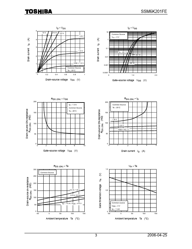
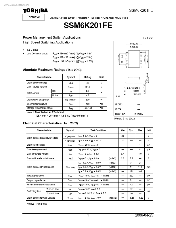
• • 1.8 V drive Low ON-resistance: Ron = 186 mΩ (max) (@VGS = 1.8V) Ron = 119 mΩ (max) (@VGS = 2.5V) Ron = 91 mΩ (max) (@VGS = 4.0V) Unit: mm
Absolute Maximum Ratings (Ta = 25°C)
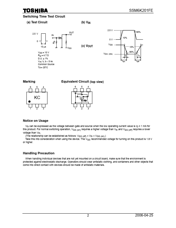
Characteristic Drain–source voltage Gate–source voltage Drain current Drain power dissipation Channel temperature Storage temperature range DC Pulse Symbol VDS VGSS ID IDP PD (Note 1) Tch Tstg Rating 20 ± 12 2.3 4.6 500 150 −55~150 Unit V V A ES6 W °C °C 1, 2, 5, 6 : Drain 3 : Gate 4 : Source
JEDEC JEITA TOSHIBA
― ― 2-2N1A
Note 1: Mounted on an FR4 board. (25.4 mm × 25.4 mm × 1.6 t, Cu Pad: 645 mm2 )
Weight: 3 mg (typ.
 SSM6K201FE Datasheet