Click to expand full text
www.DataSheet4U.com
DATASHEET
28-BIT CONFIGURABLE REGISTERED BUFFER FOR DDR2
ICSSSTUAH32868A
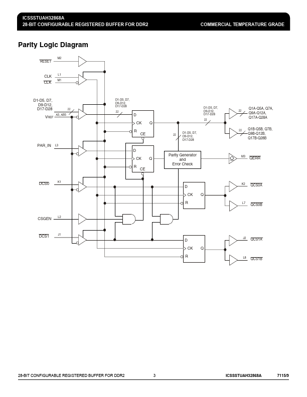
QERR pin (active low). The convention is even parity, i.e., valid parity is defined as an even number of ones across the DIMM-independent data inputs combined with the parity input bit. To calculate parity, all DIMM-independent D-inputs must be tied to a known logic state. If an error occurs and the QERR output is driven low, it stays latched low for a minimum of two clock cycles or until RESET is driven low. If two or more consecutive parity errors occur, the QERR output is driven low and latched low for a clock duration equal to the parity error duration or until RESET is driven low.
 ICSSSTUAH32868A Datasheet