Click to expand full text
www.DataSheet4U.com
DATASHEET
28-BIT 1:2 REGISTERED BUFFER WITH PARITY
IDT74SSTUBF32865A
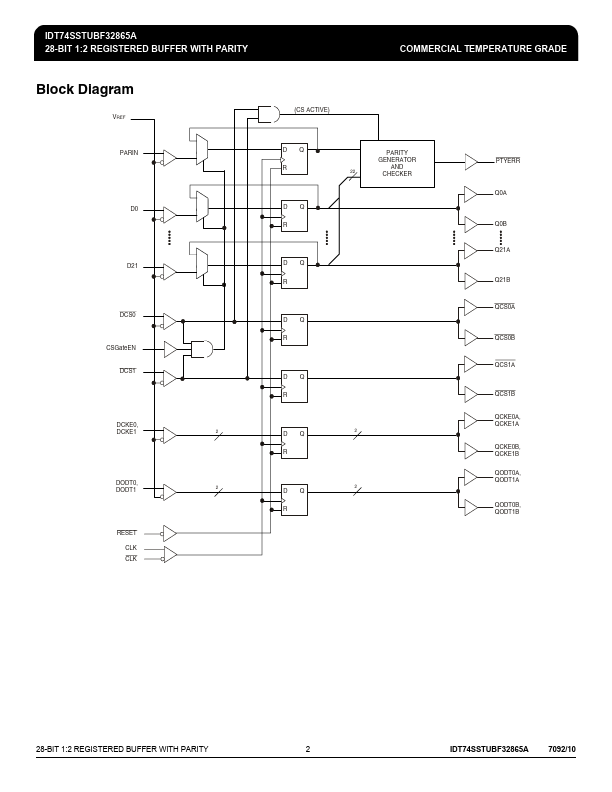
The IDT74SSTUBF32865A includes a parity checking function. The IDT74SSTUBF32865A accepts a parity bit from the memory controller at its input pin PARIN, compares it with the data received on the D-inputs and indicates whether a parity error has occurred on its open-drain PTYERR pin (active LOW).
Description
This 28-bit 1:2 registered buffer with parity is designed for 1.7V to 1.9V VDD operation. All clock and data inputs are compatible with the JEDEC standard for SSTL_18. The control inputs are LVCMOS. All outputs are 1.8 V CMOS drivers that have been optimized to drive the DDR2 DIMM load. The IDT74SSTUBF32865A operates from a differential clock (CLK and CLK).
 ICSSSTUAF32865A Datasheet