Datasheet Details
| Part number | ICSSSTU32866 |
|---|---|
| Manufacturer | Integrated Circuit System |
| File Size | 202.68 KB |
| Description | 25-Bit Configurable Registered Buffer |
| Datasheet |
 ICSSSTU32866 Datasheet ICSSSTU32866 Datasheet
|
|
|
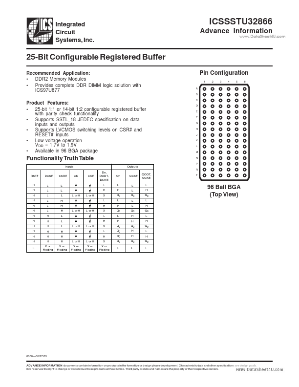
This 25-bit 1:1 or 14-bit 1:2 configurable registered buffer is designed for 1.7-V to 1.9-V VDD operation.
All clock and data inputs are compatible with the JEDEC standard for SSTL_18.
The control inputs are LVCMOS.
| Part number | ICSSSTU32866 |
|---|---|
| Manufacturer | Integrated Circuit System |
| File Size | 202.68 KB |
| Description | 25-Bit Configurable Registered Buffer |
| Datasheet |
ICSSSTU32866 Datasheet
|
|
|
|
| Part Number | Description | Manufacturer |
|---|---|---|
| ICSSSTU32864 | 25-Bit Configurable Registered Buffer | ICS |
| ICSSSTUA32S869B | 14-Bit Configurable Registered Buffer | ICS |
| ICSSSTUAF32865A | 25-BIT CONFIGURABLE REGISTERED BUFFER | IDT |
| ICSSSTUAF32866B | 25-BIT CONFIGURABLE REGISTERED BUFFER | IDT |
| ICSSSTUAF32866C | 25-BIT CONFIGURABLE REGISTERED BUFFER | IDT |
| Part Number | Description |
|---|---|
| ICS1562 | programmable differential Output Video Dot Clock Generator |
| ICS1562A | User-programmable differential Output Graphics Clock Generator |
| ICS1562B | User-programmable differential Output Graphics Clock Generator |
| ICS855011 | 1-to-2 Differential-to-2.5V/3.3V CML Fanout Buffer |
| ICS858011 | 1-TO-2 DIFFERNTIAL-TO-CML FANOUT BUFFER |