Click to expand full text
www.DataSheet4U.com
DATASHEET
25-BIT CONFIGURABLE REGISTERED BUFFER FOR DDR2
CONFIDENTIAL
IDT74SSTUBF32866B
Description
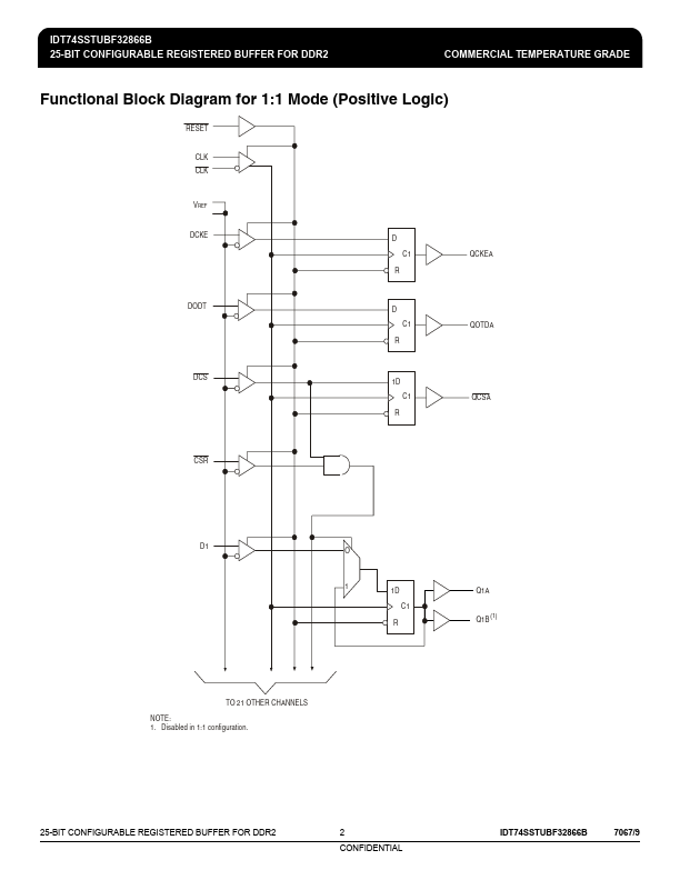
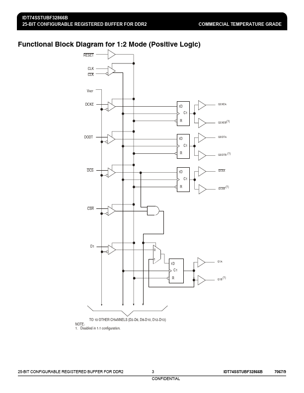
This 25-bit 1:1 or 14-bit 1:2 configurable registered buffer is designed for 1.7-V to 1.9-V VDD operation. All clock and data inputs are compatible with the JEDEC standard for SSTL_18. The control inputs are LVCMOS. All outputs are 1.8-V CMOS drivers that have been optimized to drive the DDR-II DIMM load. IDT74SSTUBF32866B operates from a differential clock (CLK and CLK). Data are registered at the crossing of CLK going high, and CLK going low. The C0 input controls the pinout configuration of the 1:2 pinout from A configuration (when low) to B configuration (when high).
 ICSSSTUAF32866B Datasheet