Datasheet Details
| Part number | ICSSSTUB32866B |
|---|---|
| Manufacturer | ICS |
| File Size | 569.97 KB |
| Description | 25-Bit Configurable Registered Buffer |
| Datasheet |
 ICSSSTUB32866B Datasheet ICSSSTUB32866B Datasheet
|
|
|
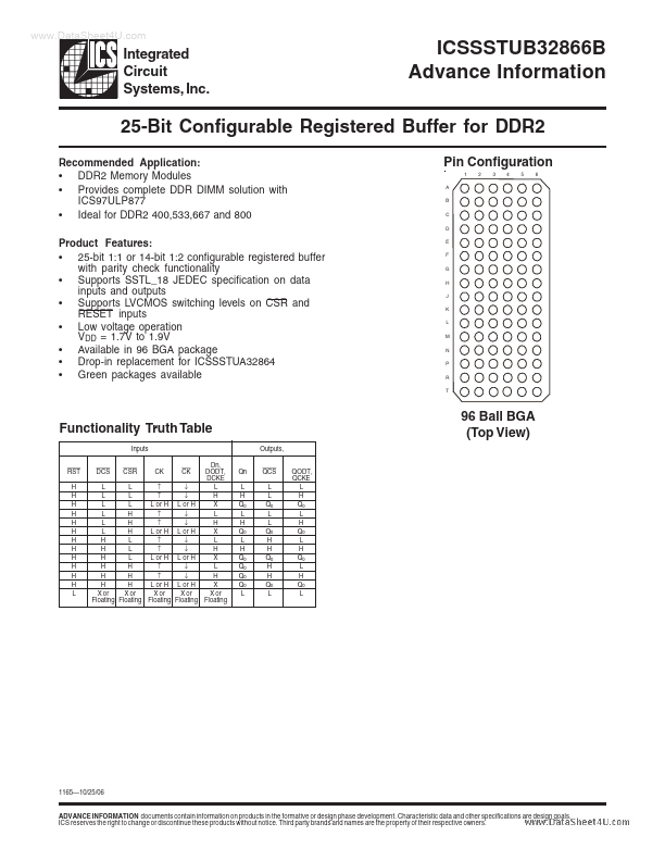
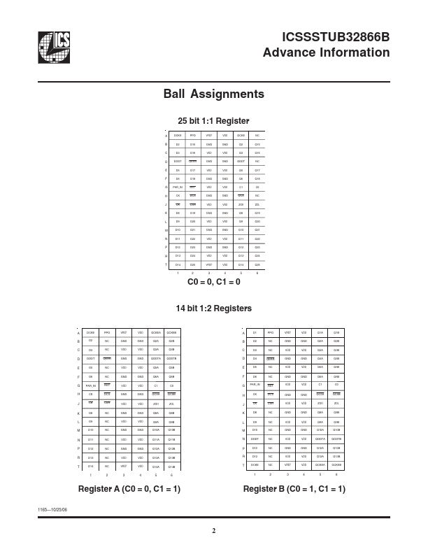
This 25-bit 1:1 or 14-bit 1:2 configurable registered buffer is designed for 1.7-V to 1.9-V VDD operation.
All clock and data inputs are compatible with the JEDEC standard for SSTL_18.
The control inputs are LVCMOS.
| Part number | ICSSSTUB32866B |
|---|---|
| Manufacturer | ICS |
| File Size | 569.97 KB |
| Description | 25-Bit Configurable Registered Buffer |
| Datasheet |
ICSSSTUB32866B Datasheet
|
|
|
|
| Part Number | Description | Manufacturer |
|---|---|---|
| ICSSSTU32866 | 25-Bit Configurable Registered Buffer | Integrated Circuit System |
| ICSSSTUAF32865A | 25-BIT CONFIGURABLE REGISTERED BUFFER | IDT |
| ICSSSTUAF32866B | 25-BIT CONFIGURABLE REGISTERED BUFFER | IDT |
| ICSSSTUAF32866C | 25-BIT CONFIGURABLE REGISTERED BUFFER | IDT |
| ICSSSTUAF32868A | 28-BIT CONFIGURABLE REGISTERED BUFFER | IDT |
| Part Number | Description |
|---|---|
| ICSSSTUB32864A | 25-Bit Configurable Registered Buffer |
| ICSSSTUB32871A | 27-Bit Registered Buffer |
| ICSSSTUB32872A | 28-Bit Registered Buffer |
| ICSSSTUBF32866A | 25-Bit Configurable Registered Buffer |
| ICSSSTU32864 | 25-Bit Configurable Registered Buffer |