Click to expand full text
www.DataSheet4U.com
DATASHEET
28-BIT CONFIGURABLE REGISTERED BUFFER FOR DDR2
CONFIDENTIAL
ICSSSTUAF32868A
Description
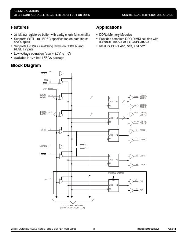
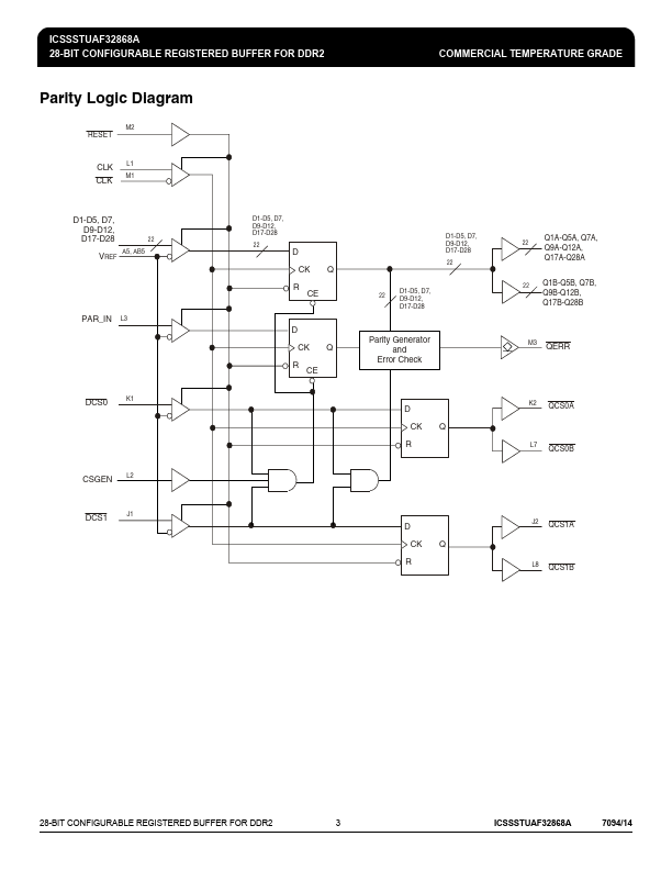
This 28-bit 1:2 configurable registered buffer is designed for 1.7V to 1.9V VDD operation. All inputs are compatible with the JEDEC standard for SSTL_18, except the chip-select gate-enable (CSGEN), control (C), and reset (RESET) inputs, which are LVCMOS. All outputs are edge-controlled circuits optimized for unterminated DIMM loads, and meet SSTL_18 specifications, except the open-drain error (QERR) output. The ICSSSTUAF32868A operates from a differential clock (CLK and CLK). Data are registered at the crossing of CLK going high and CLK going low. The device supports low-power standby operation.
 ICSSSTUAF32868A Datasheet