Datasheet4U Logo Datasheet4U.com

ICSSSTUAF32866C - 25-BIT CONFIGURABLE REGISTERED BUFFER

Description

This 25-bit 1:1 or 14-bit 1:2 configurable registered buffer is designed for 1.7-V to 1.9-V VDD operation.

All clock and data inputs are compatible with the JEDEC standard for SSTL_18.

The control inputs are LVCMOS.

Features

  • 25-bit 1:1 or 14-bit 1:2 registered buffer with parity check functionality.
  • Supports SSTL_18 JEDEC specification on data inputs and outputs.
  • Supports LVCMOS switching levels on C0, C1, and RESET inputs.
  • Low voltage operation: VDD = 1.7V to 1.9V.
  • Drop-in replacement for ICSSSTUA32864.
  • Available in 96-ball BGA package.

📥 Download Datasheet

Datasheet Details

Part number ICSSSTUAF32866C
Manufacturer IDT
File Size 669.33 KB
Description 25-BIT CONFIGURABLE REGISTERED BUFFER
Datasheet download datasheet ICSSSTUAF32866C Datasheet

Full PDF Text Transcription

Click to expand full text
www.DataSheet4U.com DATASHEET 25-BIT CONFIGURABLE REGISTERED BUFFER FOR DDR2 ICSSSTUAF32866C 
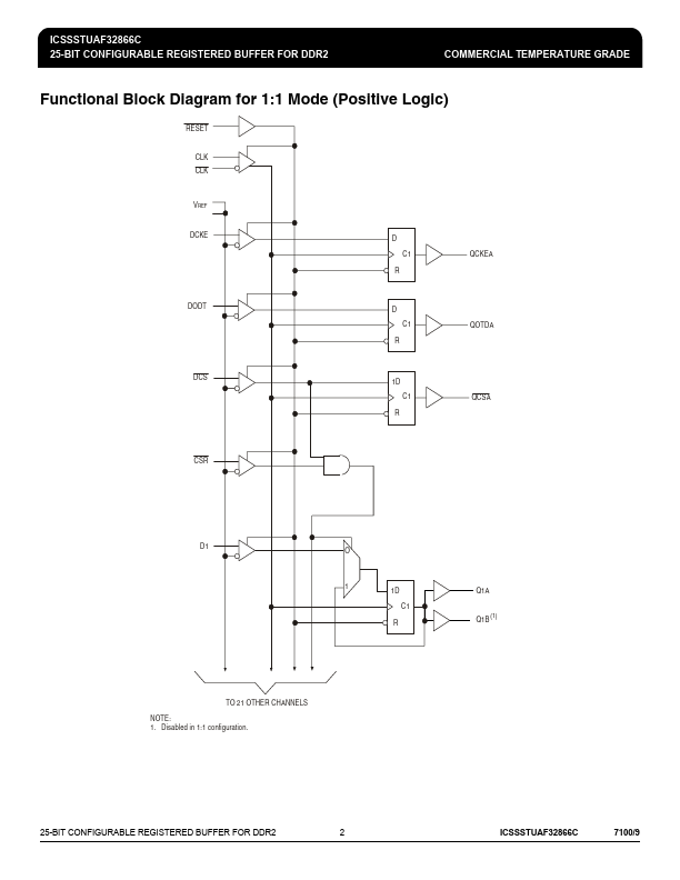
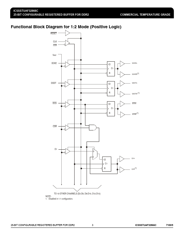
design of the ICSSSTUAF32866C must ensure that the outputs will remain low, thus ensuring no glitches on the output. The device monitors both DCS and CSR inputs and will gate the Qn outputs from changing states when both DCS and CSR inputs are high. If either DCS and CSR input is low, the Qn outputs will function normally. The RESET input has priority over the DCS and CSR control and will force the outputs low. If the DCS-control functionality is not desired, then the CSR input can be hardwired to ground, in which case, the setup-time requirement for DCS would be the same as for the other D data inputs. Package options include 96-ball LFBGA (MO-205CC).
Published: |