Datasheet Details
| Part number | AOT66919L |
|---|---|
| Manufacturer | Alpha & Omega Semiconductors |
| File Size | 284.56 KB |
| Description | 100V N-Channel MOSFET |
| Datasheet |
 AOT66919L Datasheet AOT66919L Datasheet
|
|
|
| Part number | AOT66919L |
|---|---|
| Manufacturer | Alpha & Omega Semiconductors |
| File Size | 284.56 KB |
| Description | 100V N-Channel MOSFET |
| Datasheet |
AOT66919L Datasheet
|
|
|
|
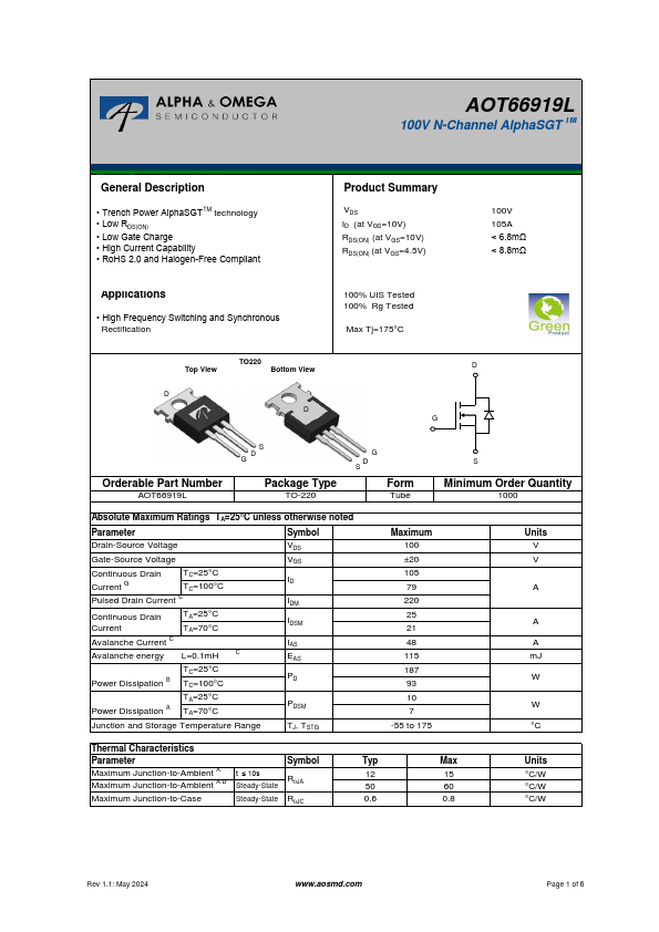
• Trench Power AlphaSGTTM technology • Low RDS(ON) • Low Gate Charge • High Current Capability • RoHS 2.0 and Halogen-Free Compliant Product Summary VDS ID (at VGS=10V) RDS(ON) (at VGS=10V) RDS(ON) (at VGS=4.5V) 100V 105A < 6.8mΩ < 8.8mΩ Applications • High Frequency Switching and Synchronous Rectification 100% UIS Tested 100% Rg Tested Max Tj=175°C Top View D TO220 Bottom View D D G Orderable Part Number AOT66919L S D G Package Type TO-220 G D S Form Tube S Minimum Order Quantity 1000 Absolute Maximum Ratings TA=25°C unless otherwise noted Parameter Symbol Drain-Source Voltage VDS Gate-Source Voltage VGS Continuous Drain Current G TC=25°C TC=100°C ID Pulsed Drain Current C IDM Continuous Drain Current TA=25°C TA=70°C IDSM Avalanche Current C IAS Avalanche energy L=0.1mH C EAS TC=25°C Power Dissipation B TC=100°C PD TA=25°C Power Dissipation A TA=70°C PDSM Junction and Storage Temperature Range TJ, TSTG Maximum 100 ±20 105 79 220 25 21 48 115 187 93 10 7 -55 to 175 Units V V A A A mJ W W °C Thermal Characteristics Parameter Symbol Typ Maximum Junction-to-Ambient A Maximum Junction-to-Ambient A D t ≤ 10s Steady-State RqJA 12 50 Maximum Junction-to-Case Steady-State RqJC 0.6 Max 15 60 0.8 Units °C/W °C/W °C/W Rev 1.1: May 2024 www.aosmd.com Page 1 of 6 AOT66919L Electrical Characteristics (TJ=25°C unless otherwise noted) Symbol Parameter Conditions Min STATIC PARAMETERS BVDSS Drain-Source Breakdown Voltage ID=250mA, VGS=0V 100 IDSS Zero Gate Voltage Drain Current VDS=100V, VGS=0V TJ=55°C IGSS Gate-Body leakage current VDS=0V, VGS=±20V VGS(th) Gate Threshold Voltage VDS=VGS, ID=250mA 1.5 VGS=10V, ID=20A RDS(ON) Static Drain-Source On-Resistance TJ=125°C VGS=4.5V, ID=20A gFS Forward Transconductance VDS=5V, ID=20A VSD Diode Forward Voltage IS=1A, VGS=0V IS Maximum Body-Diode Continuous Current G DYNAMIC PARAMETERS Ciss Input C
AOT66919L 100V N-Channel AlphaSGT TM General.
| Part Number | Description |
|---|---|
| AOT66914L | 100V N-Channel MOSFET |
| AOT66918L | 100V N-Channel MOSFET |
| AOT66518L | 150V N-Channel MOSFET |
| AOT66613L | 60V N-Channel MOSFET |
| AOT66616L | N-Channel MOSFET |
| AOT66620L | 60V N-Channel MOSFET |
| AOT66811L | 80V N-Channel MOSFET |
| AOT600A60L | 600V N-Channel Power Transistor |
| AOT600A70L | 700V N-Channel Power Transistor |
| AOT080A60L | 600V N-Channel Power Transistor |