
Datasheet Details
| Part number | AOT080A60L |
|---|---|
| Manufacturer | Alpha & Omega Semiconductors |
| File Size | 400.56 KB |
| Description | 600V N-Channel Power Transistor |
| Datasheet |
 AOT080A60L Datasheet AOT080A60L Datasheet
|

|
|
| Part number | AOT080A60L |
|---|---|
| Manufacturer | Alpha & Omega Semiconductors |
| File Size | 400.56 KB |
| Description | 600V N-Channel Power Transistor |
| Datasheet |
AOT080A60L Datasheet
|
|
|
|
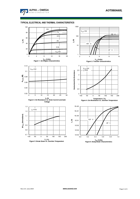
• Proprietary αMOS5TM technology • Low RDS(ON) • Optimized switching parameters for better EMI performance • Enhanced body diode for robustness and fast reverse • RreocHoSve2ry.0 and Halogen-Free Compliant Product Summary VDS @ Tj,max IDM RDS(ON),max Qg,typ Eoss @ 400V 700V 140A < 0.08Ω 70nC 9.1mJ Applications • PFC and PWM stages (LLC, PSFB,TTF) of Server, Telecom, Industrial, UPS, and Solar Inverters 100% UIS Tested 100% Rg Tested TO-220 Top View Bottom View D D Orderable Part Number AOT080A60L GDS Package Type TO-220 Green G D S Form Tube Absolute Maximum Ratings TA=25°C unless otherwise noted Parameter Symbol Drain-Source Voltage VDS Gate-Source Voltage Continuous Drain TC=25°C Current TC=100°C Pulsed Drain Current C Avalanche Current C Repetitive avalanche energy C Single pulsed avalanche energy G MOSFET dv/dt ruggedness Peak diode recovery dv/dt VGS ID IDM IAR EAR EAS dv/dt TC=25°C Power Dissipation B Derate above 25°C PD Junction and Storage Temperature Range TJ, TSTG Maximum lead temperature for soldering purpose, 1/8" from case for 5 seconds TL Maximum 600 ±20 35 22 140 11 60 690 100 20 260 2.1 -55 to 150 300 Thermal Characteristics Parameter Maximum Junction-to-Ambient A,D Maximum Case-to-sink A Maximum Junction-to-Case Symbol RqJA RqCS RqJC Maximum 65 0.5 0.48 D G S Minimum Order Quantity 1000 Units V V A A mJ mJ V/ns W W/°C °C °C Units °C/W °C/W °C/W Rev.2.0: June 2024 www.aosmd.com Page 1 of 6 AOT080A60L Electrical Characteristics (TJ=25°C unless otherwise noted) Symbol Parameter Conditions Min Typ Max Units STATIC PARAMETERS BVDSS BVDSS /∆TJ IDSS IGSS VGS(th) RDS(ON) gFS VSD IS ISM Drain-Source Breakdown Voltage Breakdown Voltage Temperature Coefficient ID=250μA, VGS=0V, TJ=25°C ID=1mA, VGS=0V, TJ=150°C ID=1mA, VGS=0V Zero Gate Voltage Drain Current VDS=600V, VGS=0V VDS=480V, TJ=125°C Gate-Body leakage current VDS=0V, VGS=±20
AOT080A60L 600V, a MOS5 TM N-Channel Power Transistor General.
| Part Number | Description |
|---|---|
| AOT095A60L | N-Channel Power Transistor |
| AOT10B60D | 10A IGBT |
| AOT10B65M1 | 10A Alpha IGBT |
| AOT10B65MQ2 | 10A AlphaIGBT |
| AOT10N60 | 10A N-Channel MOSFET |
| AOT10N65 | 10A N-Channel MOSFET |
| AOT10T60 | N-Channel MOSFET |
| AOT10T60P | N-Channel MOSFET |
| AOT1100L | 100V N-CHANNEL MOSFET |
| AOT11C60 | 11A N-Channel MOSFET |