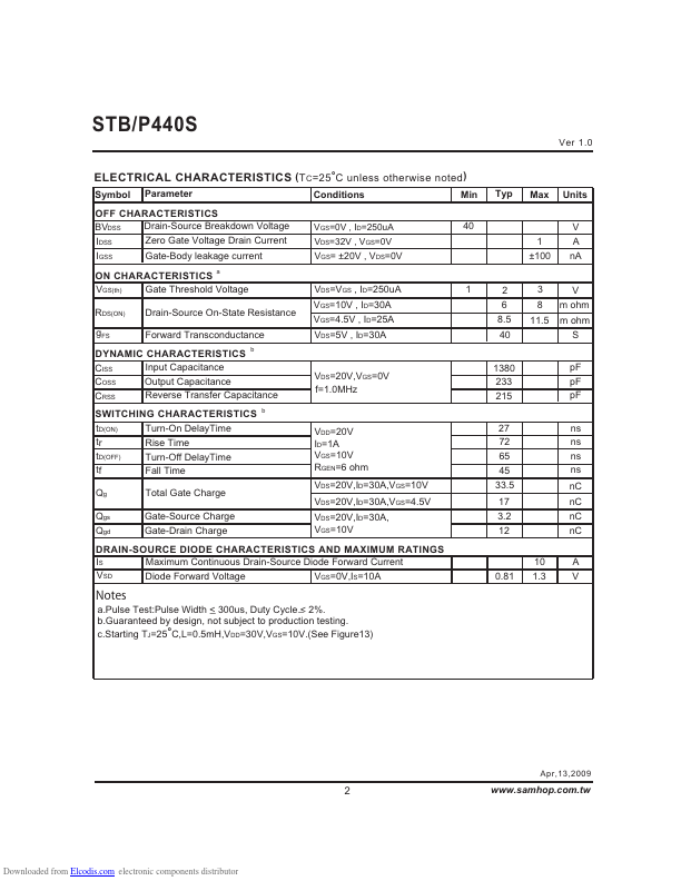
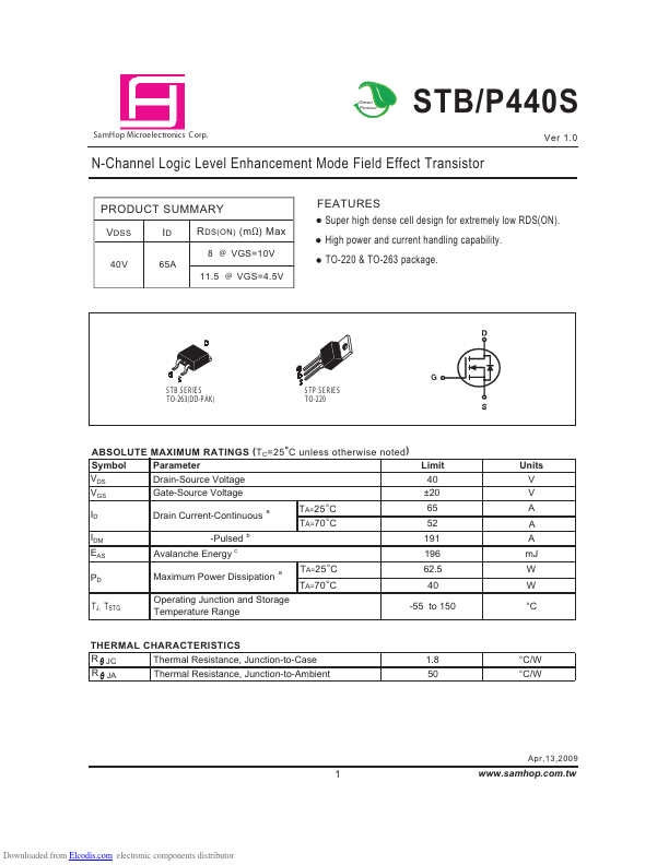
Super high dense cell design for extremely low RDS(ON). High power and current handling capability. TO-220 & TO-263 package. ID
65A
R DS(ON) (m Ω) Max
8 @ VGS=10V 11.5 @ VGS=4.5V
D
G
S
G D S
S TB S E R IE S TO-263(DD-P AK)
S TP S E R IE S TO-220.
STB40NF03L - N-CHANNEL POWER MOSFET(STMicroelectronics)
STB40NF10 - N-channel Power MOSFET(STMicroelectronics)
STB40NF10-1 - N-channel Power MOSFET(STMicroelectronics)
STB40NF10L - N-CHANNEL POWER MOSFET(STMicroelectronics)
Other Datasheets by SamHop Microelectronics
STB4410- N-Channel Logic Level Enhancement Mode Field Effect Transistor
STB432S- N-Channel Logic Enhancement Mode Field Effect Transistor
STB434S- N-Channel Logic Level Enhancement Mode Field Effect Transistor
STB438A- N-Channel Enhancement Mode Field Effect Transistor
STB438S- N-Channel Enhancement Mode Field Effect Transistor
STB1082- N-Channel Enhancement Mode Field Effect Transistor
STB10N03- N-Channel Enhancement Mode Field Effect Transistor
STB28N15- N-Channel Enhancement Mode Field Effect Transistor
Full PDF Text Transcription
Click to expand full text
Green Product
STB/P440S
Ver 1.0
S a mHop Microelectronics C orp.
N-Channel Logic Level Enhancement Mode Field Effect Transistor
PRODUCT SUMMARY
V DSS
40V
FEATURES Super high dense cell design for extremely low RDS(ON). High power and current handling capability. TO-220 & TO-263 package.
ID
65A
R DS(ON) (m Ω) Max
8 @ VGS=10V 11.5 @ VGS=4.5V
D
G
S
G D S
S TB S E R IE S TO-263(DD-P AK)
S TP S E R IE S TO-220
ABSOLUTE Symbol VDS VGS ID IDM EAS PD TJ, TSTG
MAXIMUM RATINGS ( T C=25 °C unless otherwise noted ) Parameter Drain-Source Voltage Gate-Source Voltage Drain Current-Continuous -Pulsed Avalanche Energy c Maximum Power Dissipation
a b a
Limit 40 ±20 65 52 191 196
Units V V A A A mJ W W °C
TA=25 °C TA=70 °C
TA=25 °C TA=70 °C
62.
 STB440S Datasheet