STB40N20
Features
TYPE
.. STP40N20
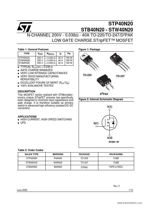
Figure 1: Package
ID 40 A 40 A 40 A Pw 160 W 160 W 160 W
3 1 2
1 2 3
VDSS 200 V 200 V 200 V
RDS(on) < 0.045 Ω < 0.045 Ω < 0.045 Ω
STW40N20 STB40N20
- -
- -
- -
TYPICAL RDS(on) = 0.038 Ω GATE CHARGE MINIMIZED VERY LOW INTRINSIC CAPACITANCES VERY GOOD MANUFACTURING REPEATIBILITY EXCELLENT FIGURE OF MERIT (RDS- Qg) 100% AVALANCHE TESTED
TO-220
TO-247
DESCRIPTION
This MOSFET series realized with STMicroelectronics unique STrip FET process has specifically been designed to minimize input capacitance and gate charge. It is therefore suitable as primary switch in advanced high-efficiency isolated DC-DC converters.
D2PAK Figure 2: Internal Schematic Diagram
APPLICATIONS
- HIGH CURRENT, HIGH SPEED SWITCHING
- UPS
Table 2: Order Codes
SALES TYPE STP40N20 STW40N20 STB40N20 MARKING P40N20 W40N20 B40N20 PACKAGE TO-220 TO-247 D2PAK PACKAGING TUBE TUBE TAPE & REEL
Rev. 3 June 2005 1/13
- STP40N20
- STW40N20
Table 3: Absolute Maximum ratings
Symbol...