STB432S
FEATURES
Super high dense cell design for extremely low RDS(ON). High power and current handling capability. TO-220 & TO-263 package.
60A
R DS(ON) (m Ω) Max
9 @ VGS=10V 11 @ VGS=4.5V
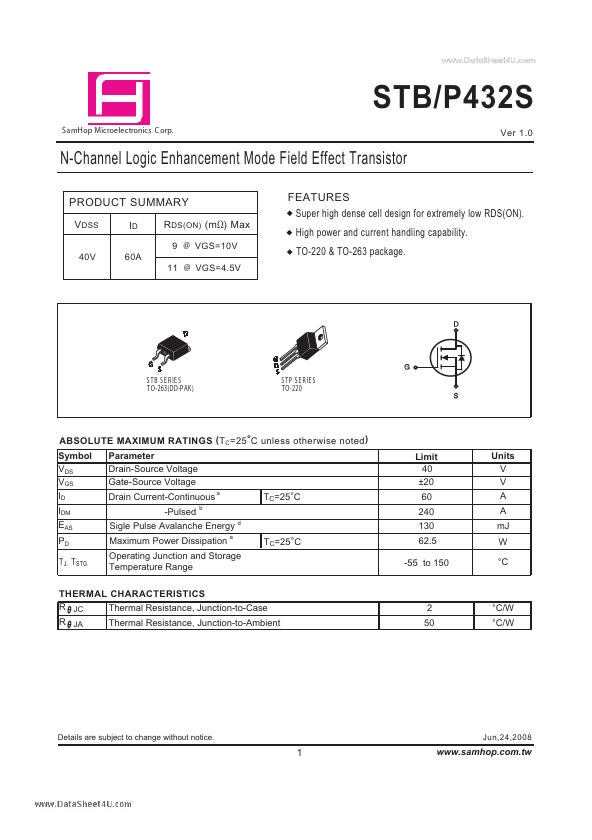
S TB S E R IE S TO-263(DD-P AK)
S TP S E R IE S TO-220
ABSOLUTE MAXIMUM RATINGS ( T C=25 °C unless otherwise noted ) Symbol VDS VGS ID IDM EAS PD TJ, TSTG Parameter Drain-Source Voltage Gate-Source Voltage Drain Current-Continuous b a
Limit 40 ±20 TC=25°C 60 240 130 TC=25°C 62.5 -55 to 150
Units V V A A m J W °C
-Pulsed Sigle Pulse Avalanche Energy d Maximum Power Dissipation a
Operating Junction and Storage Temperature Range
THERMAL CHARACTERISTICS R JC Thermal Resistance, Junction-to-Case R JA Thermal Resistance, Junction-to-Ambient
2 50
°C/W °C/W
Details are subject to change without notice.
Jun,24,2008
.samhop..tw
..
STB/P432S
Ver 1.0
ELECTRICAL CHARACTERISTICS ( T C=25 °C unless otherwise noted )
4 Symbol
Parameter
Conditions
VGS=0V , ID=250u A VDS=32V ,...