Datasheet Details
- Part number
- AS4C256M16D3LB-12BIN
- Manufacturer
- Alliance Semiconductor
- File Size
- 2.37 MB
- Datasheet
- AS4C256M16D3LB-12BIN-AllianceSemiconductor.pdf
- Description
- 4Gb DRAM
AS4C256M16D3LB-12BIN Description
AS4C256M16D3LB-12BIN AS4C256M16D3LB-12BCN Revision History 4Gb AS4C256M16D3LB - 12BIN/BCN 96 ball FBGA PACKAGE Revision Rev 1.0 Rev 1.1 Details Pre.
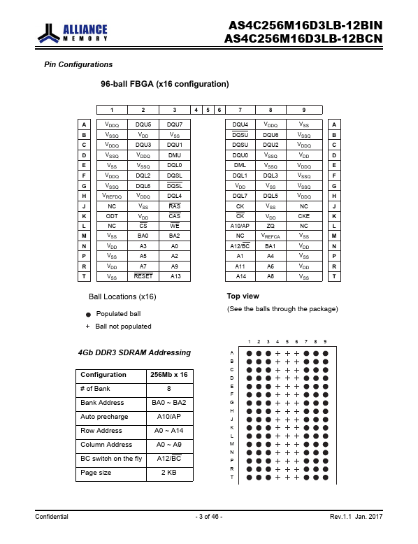
Pin
CK, CK CKE
CS ODT
RAS, CAS, WE DM
(DMU), (DML)
Type
Input Input
Input Input
Input Input
Function
Clock : CK and CK are differential clock input.
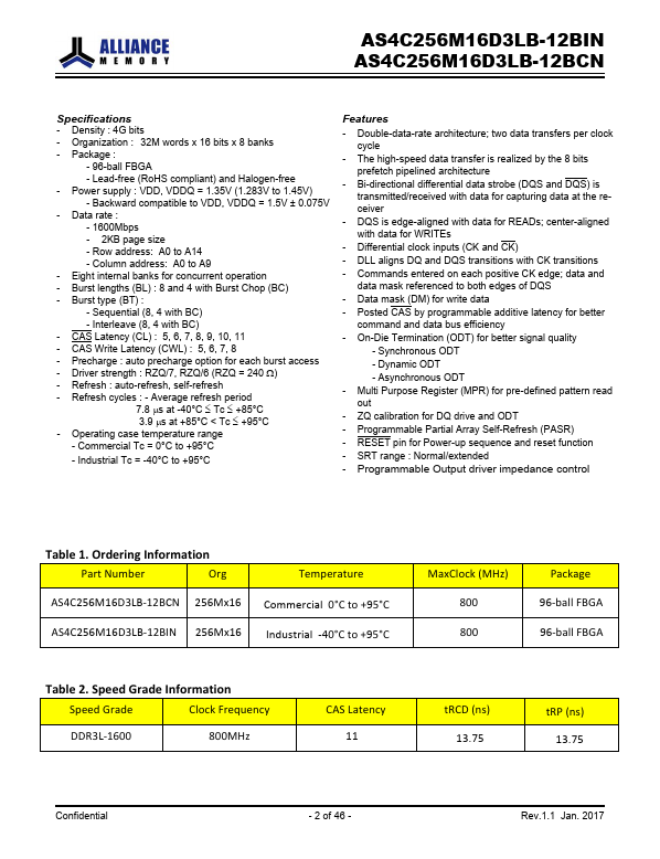
AS4C256M16D3LB-12BIN Features
* - Double-data-rate architecture; two data transfers per clock cycle
- The high-speed data transfer is realized by the 8 bits prefetch pipelined architecture
- Bi-directional differential data strobe (DQS and DQS) is transmitted/received with data for capturing data at the receiver
- DQS is edge-alig
📁 Related Datasheet
📌 All Tags