Datasheet Details
- Part number
- AS4C256M16D3LB-12BAN
- Manufacturer
- Alliance Semiconductor
- File Size
- 1.88 MB
- Datasheet
- AS4C256M16D3LB-12BAN-AllianceSemiconductor.pdf
- Description
- 4Gb DRAM
AS4C256M16D3LB-12BAN Description
AS4C256M16D3LB-12BAN Revision History 4Gb AS4C256M16D3LB - 12BAN 96 ball FBGA PACKAGE Revision Details Rev 1.0 Preliminary datasheet Date Mar.2018 .
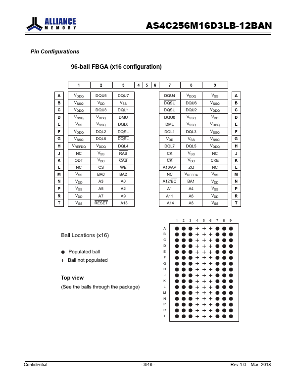
Pin
CK, CK CKE
CS ODT
RAS, CAS, WE DM
(DMU), (DML)
Type
Input Input
Input Input
Input Input
Function
Clock : CK and CK are differential clock input.
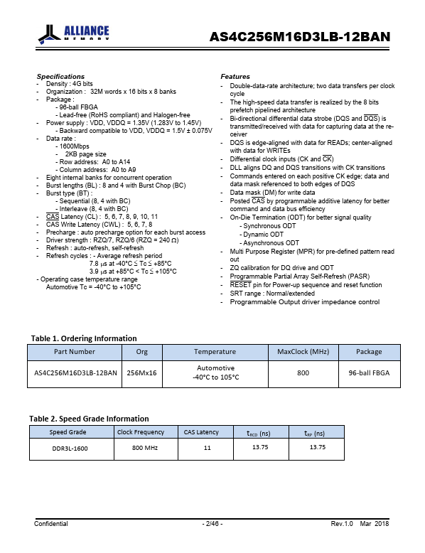
AS4C256M16D3LB-12BAN Features
* - Double-data-rate architecture; two data transfers per clock cycle
- The high-speed data transfer is realized by the 8 bits prefetch pipelined architecture
- Bi-directional differential data strobe (DQS and DQS) is transmitted/received with data for capturing data at the receiver
- DQS is edge-alig
📁 Related Datasheet
📌 All Tags