CGHV27100
CGHV27100 is GaN HEMT manufactured by Cree.
100 W, 2500-2700 MHz, 50 V, GaN HEMT for LTE
Cree’s CGHV27100 is a gallium nitride (GaN) high electron mobility transistor (HEMT) is designed specifically for high efficiency, high gain and wide bandwidth capabilities, which makes the CGHV27100 ideal for 2.5
- 2.7 GHz LTE, 4G Tele and BWA amplifier applications. The transistor is input matched and supplied in a ceramic/ metal pill and flange packages.
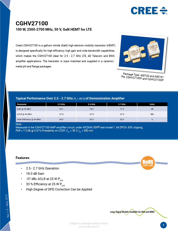
PNPa: CckGaHgVe2T7y1p0e0: F44a0n1d6C2GaHndV2474100106P1
Typical Performance Over 2.5
- 2.7 GHz (TC = 25˚C) of Demonstration Amplifier
Parameter
2.5 GHz
2.6 GHz
2.7 GHz
Gain @ 44 dBm
ACLR @ 44 dBm
-37.0
-37.0
-37.0
Drain Efficiency @ 44...