Part number:
CGHV22200
Manufacturer:
Cree
File Size:
769.10 KB
Description:
Gan hemt.
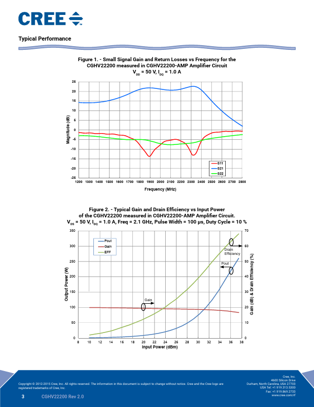
CGHV22200 Features
* 1.8 - 2.2 GHz Operation
* 18 dB Gain
* -35 dBc ACLR at 50 W PAVE
* 31-35 % Efficiency at 50 W PAVE
* High Degree of DPD Correction Can be Applied Rev 1.0
* May 2015 Subject to change without notice. www.cree.com/rf 1 Absolute Maximum Ratings
CGHV22200 Datasheet (769.10 KB)
Datasheet Details
CGHV22200
Cree
769.10 KB
Gan hemt.
📁 Related Datasheet
CGHV22100 GaN HEMT (Cree)
CGHV27015S GaN HEMT (Cree)
CGHV27015S GaN HEMT (Wolfspeed)
CGHV27030S GaN HEMT (CREE)
CGHV27030S GaN HEMT (MACOM)
CGHV27060MP GaN HEMT (Cree)
CGHV27100 GaN HEMT (Cree)
CGHV27200 GaN HEMT (Cree)
CGHV22200 Distributor