Datasheet4U Logo Datasheet4U.com

CDCVF25081 - 3.3-V Phased-Lock Loop Clock Driver

Datasheet Summary

Description

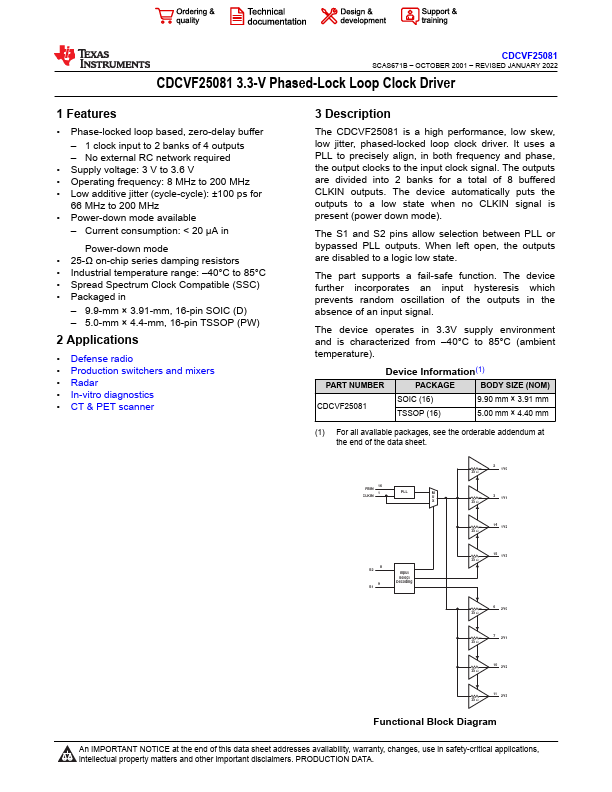
The CDCVF25081 is a high performance, low skew, low jitter, phased-locked loop clock driver.

It uses a PLL to precisely align, in both frequency and phase, the output clocks to the input clock signal.

The outputs are divided into 2 banks for a total of 8 buffered CLKIN outputs.

Features

  • Phase-locked loop based, zero-delay buffer.
  • 1 clock input to 2 banks of 4 outputs.
  • No external RC network required.
  • Supply voltage: 3 V to 3.6 V.
  • Operating frequency: 8 MHz to 200 MHz.
  • Low additive jitter (cycle-cycle): ±100 ps for 66 MHz to 200 MHz.
  • Power-down mode available.
  • Current consumption: < 20 µA in Power-down mode.
  • 25-Ω on-chip series damping resistors.
  • Industrial temperature range:.
  • 40°C.

📥 Download Datasheet

Datasheet preview – CDCVF25081

Datasheet Details

Part number CDCVF25081
Manufacturer Texas Instruments
File Size 1.18 MB
Description 3.3-V Phased-Lock Loop Clock Driver
Datasheet download datasheet CDCVF25081 Datasheet
Additional preview pages of the CDCVF25081 datasheet.
Other Datasheets by Texas Instruments

Full PDF Text Transcription

Click to expand full text
CDCVF25081 SCAS671B – OCTOBER 2001 – REVISED JANUARY 2022 CDCVF25081 3.3-V Phased-Lock Loop Clock Driver 1 Features • Phase-locked loop based, zero-delay buffer – 1 clock input to 2 banks of 4 outputs – No external RC network required • Supply voltage: 3 V to 3.6 V • Operating frequency: 8 MHz to 200 MHz • Low additive jitter (cycle-cycle): ±100 ps for 66 MHz to 200 MHz • Power-down mode available – Current consumption: < 20 µA in Power-down mode • 25-Ω on-chip series damping resistors • Industrial temperature range: –40°C to 85°C • Spread Spectrum Clock Compatible (SSC) • Packaged in – 9.9-mm × 3.91-mm, 16-pin SOIC (D) – 5.0-mm × 4.
Published: |