Datasheet4U Logo Datasheet4U.com

Si53208 - Low Power Gen 1/2/3/4/5 Clock Buffer

This page provides the datasheet information for the Si53208, a member of the Si53212 Low Power Gen 1/2/3/4/5 Clock Buffer family.

Features

  • 12/8/4-output 100 MHz PCIe Gen1/2/3/4/5compliant clock fanout buffer.
  • Low additive jitter: 0.02 ps rms max, Gen 5.
  • Low-power, push-pull, HCSL compatible differential outputs.
  • 10 MHz to 200 MHz clock input.
  • Individual hardware control pins and I2C controls for Output Enable.
  • Spread spectrum tolerant to pass through a spread input clock for EMI reduction.
  • Supports Intel QPI/UPI standards.
  • Single 1.5 to 1.8 V power supply.

📥 Download Datasheet

Datasheet preview – Si53208

Datasheet Details

Part number Si53208
Manufacturer Silicon Laboratories
File Size 868.87 KB
Description Low Power Gen 1/2/3/4/5 Clock Buffer
Datasheet download datasheet Si53208 Datasheet
Additional preview pages of the Si53208 datasheet.
Other Datasheets by Silicon Laboratories

Full PDF Text Transcription

Click to expand full text
Si53212/Si53208/Si53204 Data Sheet 12/8/4-Output PCI-Express Low Jitter, Low Power Gen 1/2/3/4/5 Clock Buffer 
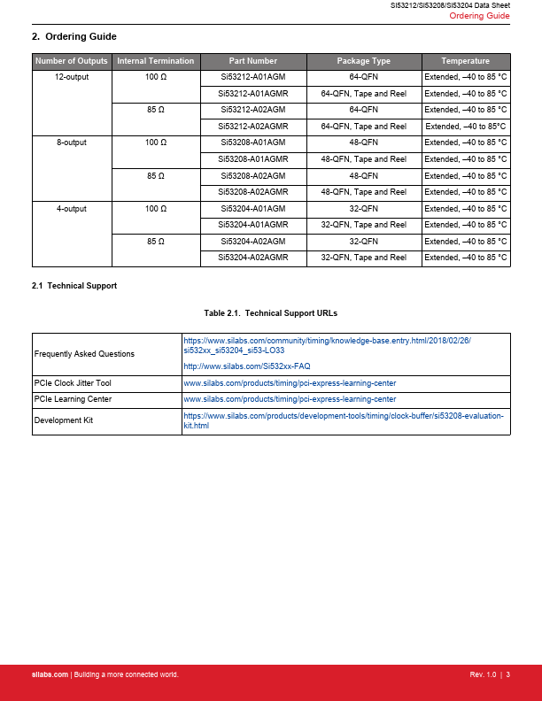
The Si53212, Si53208, and Si53204 are the industry’s highest performance, low additive jitter, low power PCIe clock fanout buffer family that can source 12, 8, or 4 clock outputs. All differential clock outputs are compliant to PCIe Gen1/2/3/4/5 common clock and separate reference clock specifications. This family of buffers is spread spectrum tolerant to pass through a spread input clock. Each device has an individual hardware output enable control pin for enabling and disabling each differential output. The device can also support input frequencies from 10 MHz to 200 MHz. All the devices are packaged in small QFN packages.
Published: |