Click to expand full text
SMD Type
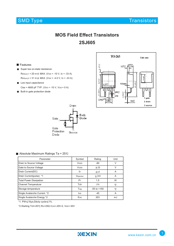
MOS Field Effect Transistors 2SJ605
TO-263
+ 0 .1 1 .2 7 -0 .1
Transistors IC
Unit: mm
+0.1 1.27-0.1 +0.2 4.57-0.2
Features
Super low on-state resistance: RDS(on)1 = 20 m RDS(on)2 = 31 m MAX. (VGS = -10 V, ID = -33 A)
+ 0 .2 8 .7 -0 .2
MAX. (VGS = -4.0 V, ID = -33 A)
Low input capacitance Ciss = 4600 pF TYP. (VDS = -10 V, VGS = 0 A)
+0.1 1.27-0.1
0.1max
+0.1 0.81-0.1
2.54
+0.2 -0.2 +0.1 5.08-0.1
+ 0 .2 2 .5 4 -0 .2
Built-in gate protection diode
+ 0 .2 5 .2 8 -0 .2
+ 0 .2 1 5 .2 5 -0 .2
2.54
+0.2 0.4-0.2
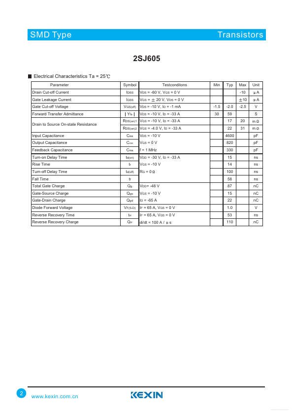
Absolute Maximum Ratings Ta = 25
Parameter Drain to Source Voltage Gate to Source Voltage Drain Current(DC) Drain Current(pulse) *1 Total Power Dissipation Channel Temperature Storage temperature Single Avalanche Current *2 Single Avalanche Energy *2 *1.
 2SJ605 Datasheet