Click to expand full text
SMD Type
MOS Field Effect Transistor 2SJ602
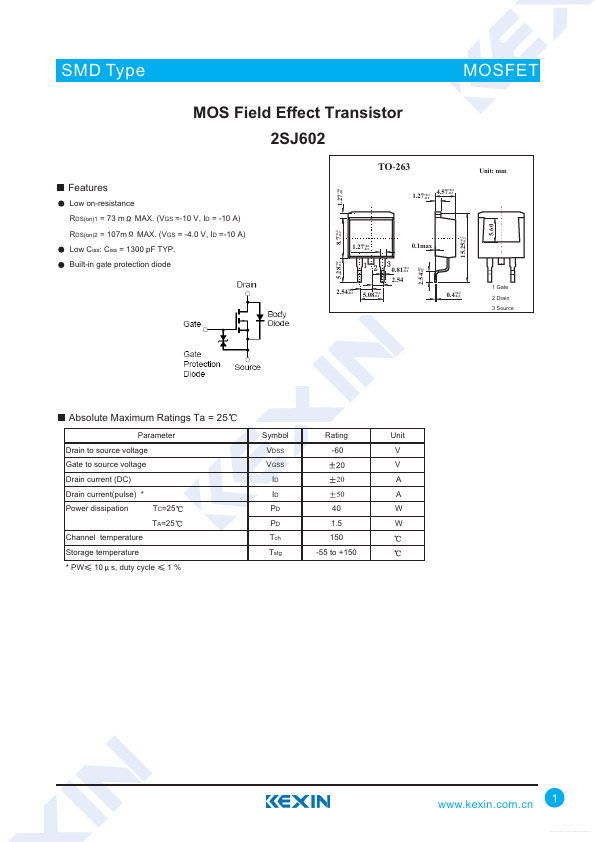
TO-263
+0.1 1.27-0.1
MOSFET
Unit: mm
+0.1 1.27-0.1 +0.2 4.57-0.2
Features
Low on-resistance RDS(on)1 = 73 m RDS(on)2 = 107m MAX. (VGS =-10 V, ID = -10 A)
Low Ciss: Ciss = 1300 pF TYP. Built-in gate protection diode
+0.2 5.28-0.2
+0.1 1.27-0.1
0.1max
+0.1 0.81-0.1
2.54 5.08
+0.1 -0.1
+0.2 2.54-0.2
+0.2 15.25-0.2
MAX. (VGS = -4.0 V, ID =-10 A)
+0.2 8.7-0.2
+0.2 2.54-0.2
+0.2 0.4-0.2
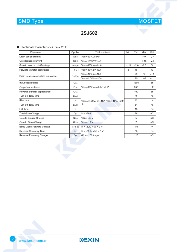
Absolute Maximum Ratings Ta = 25
Parameter Drain to source voltage Gate to source voltage Drain current (DC) Drain current(pulse) * Power dissipation TC=25 TA=25 Channel temperature Storage temperature * PW 10 s, duty cycle 1% Symbol VDSS VGSS ID ID PD PD Tch Tstg Rating -60 20 20 50 40 1.5 150 -55 to +150 Unit V V A A W W
5.
 2SJ602 Datasheet