Datasheet Details
| Part number | ICSSSTUF32864A |
|---|---|
| Manufacturer | Integrated Circuit Systems |
| File Size | 111.62 KB |
| Description | 25-Bit Configurable Registered Buffer for DDR2 |
| Datasheet |
 ICSSSTUF32864A Datasheet ICSSSTUF32864A Datasheet
|
|
|
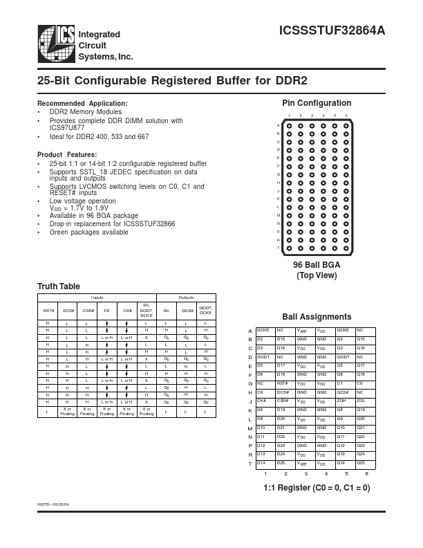
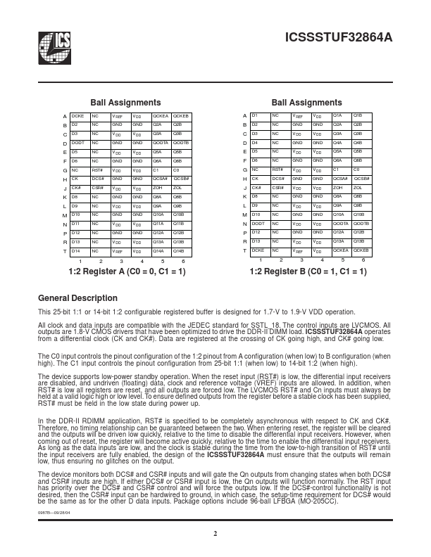
This 25-bit 1:1 or 14-bit 1:2 configurable registered buffer is designed for 1.7-V to 1.9-V VDD operation.
All clock and data inputs are compatible with the JEDEC standard for SSTL_18.
The control inputs are LVCMOS.
| Part number | ICSSSTUF32864A |
|---|---|
| Manufacturer | Integrated Circuit Systems |
| File Size | 111.62 KB |
| Description | 25-Bit Configurable Registered Buffer for DDR2 |
| Datasheet |
ICSSSTUF32864A Datasheet
|
|
|
|
| Part Number | Description | Manufacturer |
|---|---|---|
| ICSSSTU32864 | 25-Bit Configurable Registered Buffer | ICS |
| ICSSSTU32866 | 25-Bit Configurable Registered Buffer | Integrated Circuit System |
| ICSSSTUA32S869B | 14-Bit Configurable Registered Buffer | ICS |
| ICSSSTUAF32865A | 25-BIT CONFIGURABLE REGISTERED BUFFER | IDT |
| ICSSSTUAF32866B | 25-BIT CONFIGURABLE REGISTERED BUFFER | IDT |
| Part Number | Description |
|---|---|
| ICSSSTV16857 | DDR 14-Bit Registered Buffer |
| ICSSSTV16859 | DDR 13-Bit to 26-Bit Registered Buffer |
| ICSSSTV32852 | DDR 24-Bit to 48-Bit Registered Buffer |
| ICSSSTVA16857 | DDR 14-Bit Registered Buffer |
| ICSSSTVA16859B | DDR 13-Bit to 26-Bit Registered Buffer |