Datasheet Details
| Part number | ICSSSTV32852 |
|---|---|
| Manufacturer | Integrated Circuit Systems |
| File Size | 146.82 KB |
| Description | DDR 24-Bit to 48-Bit Registered Buffer |
| Datasheet |
 ICSSSTV32852 Datasheet ICSSSTV32852 Datasheet
|
|
|
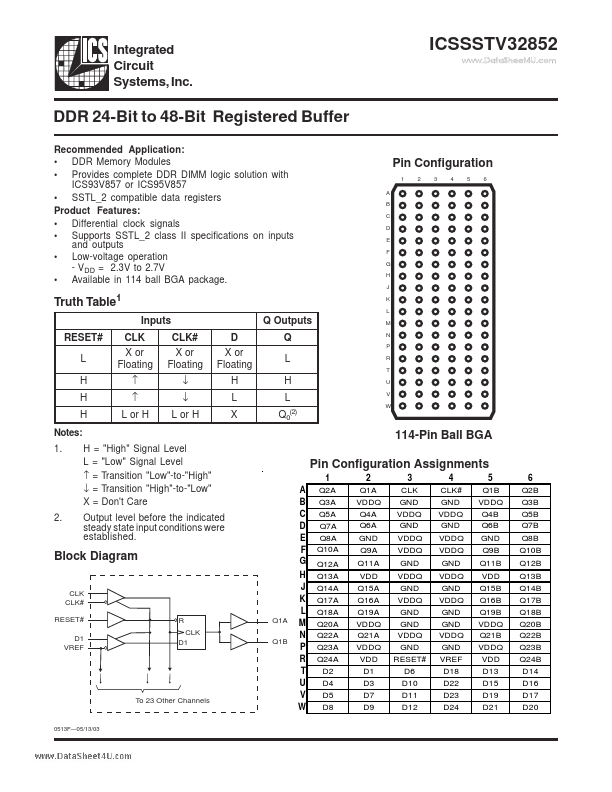
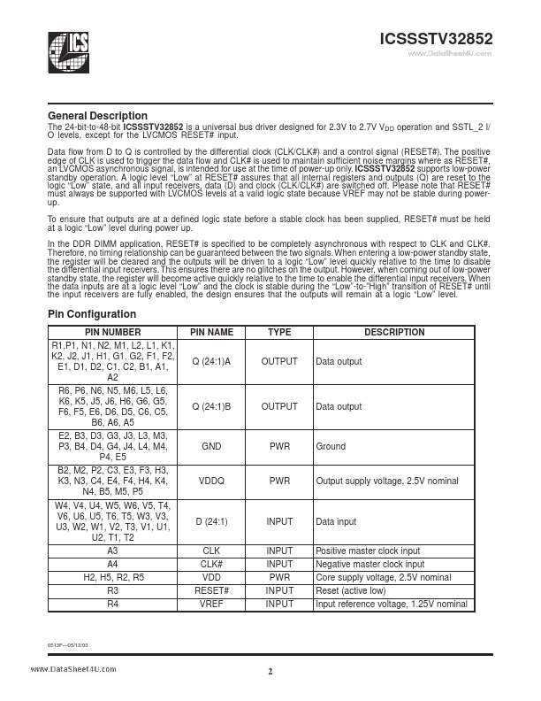
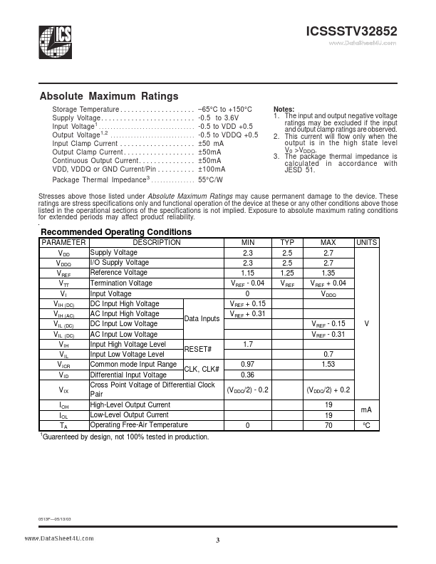
The 24-bit-to-48-bit ICSSSTV32852 is a universal bus driver designed for 2.3V to 2.7V VDD operation and SSTL_2 I/ O levels, except for the LVCMOS RESET# input.
Data flow from D to Q is controlled by the differential clock (CLK/CLK#) and a control signal (RESET#).
| Part number | ICSSSTV32852 |
|---|---|
| Manufacturer | Integrated Circuit Systems |
| File Size | 146.82 KB |
| Description | DDR 24-Bit to 48-Bit Registered Buffer |
| Datasheet |
ICSSSTV32852 Datasheet
|
|
|
|
| Part Number | Description | Manufacturer |
|---|---|---|
| ICSSSTVA16859C | DDR 13-Bit to 26-Bit Registered Buffer | Renesas |
| ICSSSTVA16859C | DDR 13-Bit to 26-Bit Registered Buffer | IDT |
| ICSSSTVF16857 | DDR 14-Bit Registered Buffer | Renesas |
| ICSSSTU32864 | 25-Bit Configurable Registered Buffer | ICS |
| ICSSSTU32866 | 25-Bit Configurable Registered Buffer | Integrated Circuit System |
| Part Number | Description |
|---|---|
| ICSSSTV16857 | DDR 14-Bit Registered Buffer |
| ICSSSTV16859 | DDR 13-Bit to 26-Bit Registered Buffer |
| ICSSSTVA16857 | DDR 14-Bit Registered Buffer |
| ICSSSTVA16859B | DDR 13-Bit to 26-Bit Registered Buffer |
| ICSSSTVF16859 | DDR 13-Bit to 26-Bit Registered Buffer |