Datasheet Details
| Part number | AOWF12N60 |
|---|---|
| Manufacturer | Alpha & Omega Semiconductors |
| File Size | 284.28 KB |
| Description | 12A N-Channel MOSFET |
| Datasheet |
 AOWF12N60 Datasheet AOWF12N60 Datasheet
|
|
|
Download the AOWF12N60 datasheet PDF. This datasheet also includes the AOW12N60 variant, as both parts are published together in a single manufacturer document.
| Part number | AOWF12N60 |
|---|---|
| Manufacturer | Alpha & Omega Semiconductors |
| File Size | 284.28 KB |
| Description | 12A N-Channel MOSFET |
| Datasheet |
AOWF12N60 Datasheet
|
|
|
|
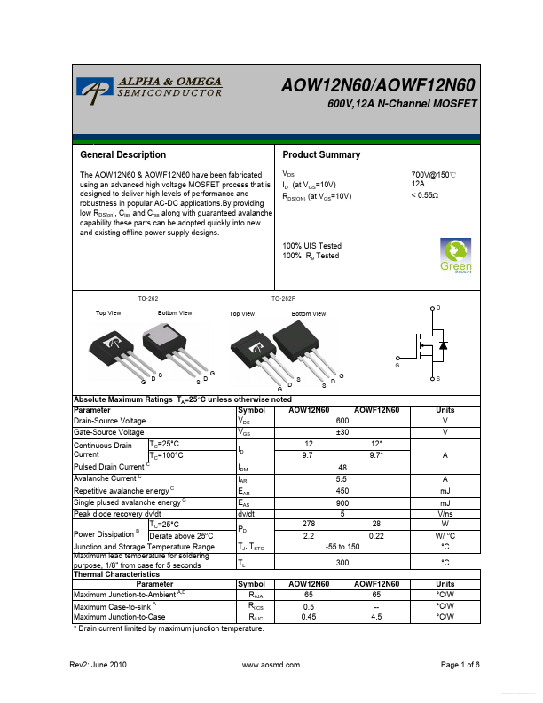
The AOW12N60 & AOWF12N60 have been fabricated using an advanced high voltage MOSFET process that is designed to deliver high levels of performance and robustness in popular AC-DC applications.By providing low RDS(on), Ciss and Crss along with guaranteed avalanche capability these parts can be adopted quickly into new and existing offline power supply designs.
Product Summary VDS ID (at VGS=10V) RDS(ON) (at VGS=10V) 700V@150℃ 12A < 0.55Ω 100% UIS Tested 100% Rg Tested TO-262 Top View Bottom View Top View TO-262F Bottom View D G G D S S D G G D S S D G S Absolute Maximum Ratings TA=25°C unless otherwise noted AOWF12N60 Symbol Parameter AOW12N60 VDS Drain-Source Voltage 600 VGS Gate-Source Voltage ±30 Continuous Drain Current Avalanche Current C Repetitive avalanche energy C Units V V A A mJ mJ V/ns W W/ oC °C °C TC=25°C TC=100°C ID IDM IAR EAR EAS dv/dt PD TJ, TSTG TL Symbol RθJA RθCS RθJC 12 9.7 48 5.5 450 900 5 278 2.2 -55 to 150 300 AOW12N60 65 0.5 0.45 12* 9.7* Pulsed Drain Current C Single plused avalanche energy G Peak diode recovery dv/dt TC=25°C Power Dissipation B Derate above 25oC Junction and Storage Temperature Range Maximum lead temperature for soldering purpose, 1/8" from case for 5 seconds Thermal Characteristics Parameter Maximum Junction-to-Ambient A,D 28 0.22 AOWF12N60 65 -4.5 Units °C/W °C/W °C/W Maximum Case-to-sink A Maximum Junction-to-Case * Drain current limited by maximum junction temperature.
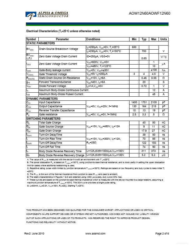
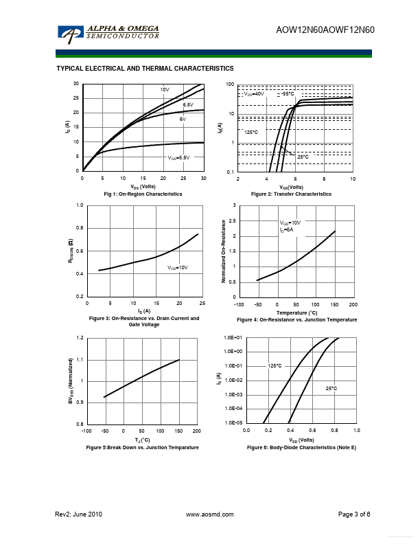
Rev2: June 2010 www.aosmd.com Page 1 of 6 Free Datasheet http://www.datasheet4u.com/ AOW12N60AOWF12N60 Electrical Characteristics (TJ=25°C unless otherwise noted) Symbol STATIC PARAMETERS BVDSS BVDSS /∆TJ IDSS IGSS VGS(th) RDS(ON) gFS VSD IS ISM Drain-Source Breakdown Voltage Zero Gate Voltage Drain Current Zero Gate Voltage Drain Current Gate-Body leakage current Gate Threshold Voltage Static Drain-Source On-Resistance Forward Transconductance Diode Forward Voltage
AOW12N60/AOWF12N60 600V,12A N-Channel MOSFET General.
| Part Number | Description |
|---|---|
| AOWF12N65 | 12A N-Channel MOSFET |
| AOWF12N50 | 12A N-Channel MOSFET |
| AOWF125A60 | N-Channel Power Transistor |
| AOWF12T60 | 12A N-Channel MOSFET |
| AOWF10N60 | 10A N-Channel MOSFET |
| AOWF10N65 | 10A N-Channel MOSFET |
| AOWF10T60 | 10A N-Channel MOSFET |
| AOWF11C60 | 11A N-Channel MOSFET |
| AOWF11S60 | Power Transistor |
| AOWF11S65 | Power Transistor |