Click to expand full text
SSC8329GS1
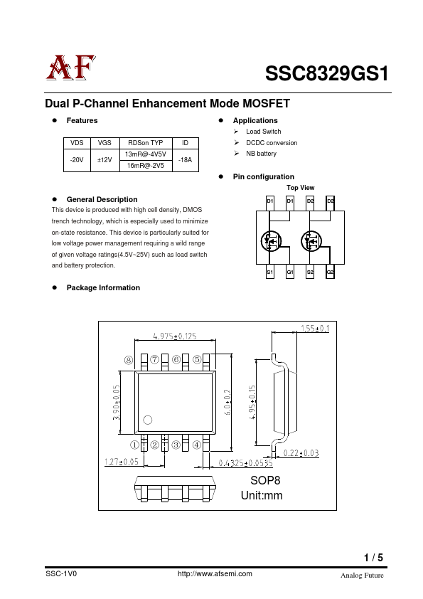
Dual P-Channel Enhancement Mode MOSFET
Features
VDS -20V
VGS ±12V
RDSon TYP 13mR@-4V5V 16mR@-2V5
ID -18A
Applications
Load Switch
DCDC conversion NB battery
Pin configuration
General Description
This device is produced with high cell density, DMOS
Top View
D1 D1 D2
trench technology, which is especially used to minimize
on-state resistance. This device is particularly suited for
low voltage power management requiring a wild range
of given voltage ratings(4.5V~25V) such as load switch
and battery protection.
S1 G1 S2
Package Information
D2 G2
⑧ ⑦ ⑥⑤
①② ③ ④
SOP8 Unit:mm
SSC-1V0
http://www.afsemi.
 SSC8329GS1 Datasheet