Datasheet Details
- Part number
- HY57V281620ELT
- Manufacturer
- Hynix Semiconductor
- File Size
- 120.33 KB
- Datasheet
- HY57V281620ELT_HynixSemiconductor.pdf
- Description
- Synchronous DRAM Memory
HY57V281620ELT Description
128Mb Synchronous DRAM based on 2M x 4Bank x16 I/O Document Title 4Bank x 2M x 16bits Synchronous DRAM Revision History Revision No.1.0 1.1 First Ve.HY57V281620ELT Features
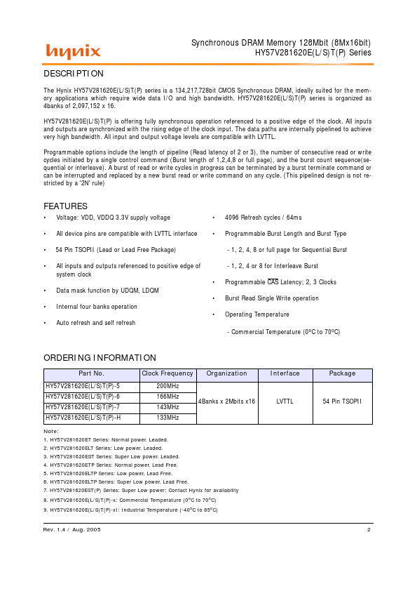
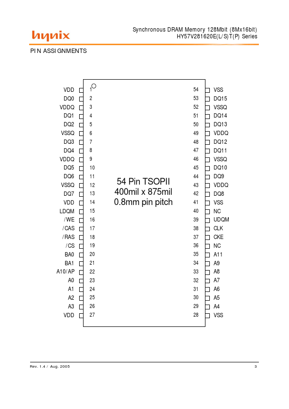
* Voltage: VDD, VDDQ 3.3V supply voltage All device pins are compatible with LVTTL interface 54 Pin TSOPII (Lead or Lead Free Package) All inputs and outputs referenced to positive edge of system clock Data mask function by UDQM, LDQMHY57V281620ELT Applications
* which require wide data I/O and high bandwidth. HY57V281620E(L)T(P) series is organized as 4banks of 2,097,152 x 16. HY57V281620E(L)T(P) is offering fully synchronous operation referenced to a positive edge of the clock. All inputs and outputs are synchronized with the rising edge of the clock input
📁 Related Datasheet
📌 All Tags