Datasheet Details
| Part number | CY7C1440AV33 |
|---|---|
| Manufacturer | Cypress Semiconductor |
| File Size | 417.46 KB |
| Description | (CY7C144xAV33) Sync SRAM |
| Datasheet |
 CY7C1440AV33_CypressSemiconductor.pdf CY7C1440AV33_CypressSemiconductor.pdf
|
| Part number | CY7C1440AV33 |
|---|---|
| Manufacturer | Cypress Semiconductor |
| File Size | 417.46 KB |
| Description | (CY7C144xAV33) Sync SRAM |
| Datasheet |
CY7C1440AV33_CypressSemiconductor.pdf
|
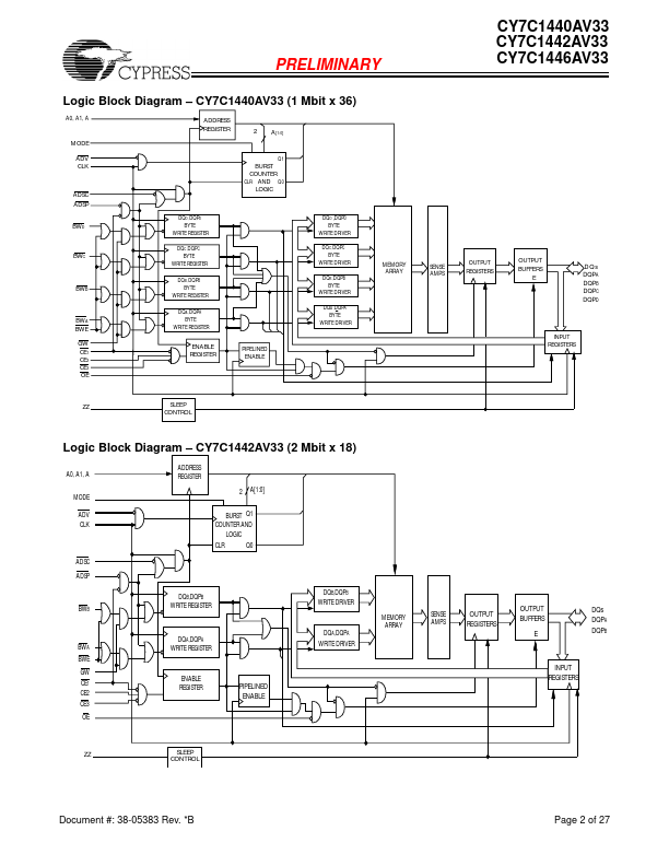
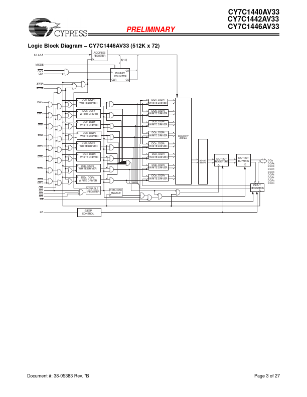
1] The CY7C1440AV33/CY7C1442AV33/CY7C1446AV33 SRAM integrates 1,048,576 x 36, 2,097,152 x 18 and 524,288 x 72 SRAM cells with advanced synchronous peripheral circuitry and a two-bit counter for internal burst operation.All synchronous inputs are gated by registers controlled by a positive-edge-triggered Clock Input (CLK).The synchronous inputs include all addresses, all data inputs, address-pipelining Chip Enable (CE1), depth-expansion Chip Enables (CE2 and CE3[2]), Burst Control inputs (ADSC,
📁 CY7C1440AV33 Similar Datasheet