Datasheet Details
| Part number | LMK00301 |
|---|---|
| Manufacturer | Texas Instruments |
| File Size | 2.13 MB |
| Description | 3-GHz 10-Output Ultra-Low Additive Jitter Differential Clock Buffer and Level Translator |
| Datasheet |
 LMK00301 Datasheet LMK00301 Datasheet
|
|
|
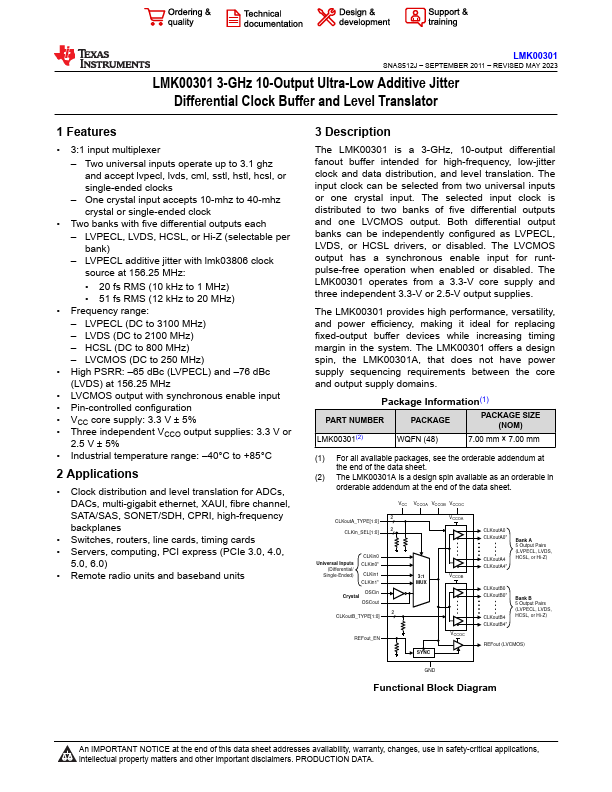
The LMK00301 is a 3-GHz, 10-output differential fanout buffer intended for high-frequency, low-jitter clock and data distribution, and level translation.
The input clock can be selected from two universal inputs or one crystal input.
| Part number | LMK00301 |
|---|---|
| Manufacturer | Texas Instruments |
| File Size | 2.13 MB |
| Description | 3-GHz 10-Output Ultra-Low Additive Jitter Differential Clock Buffer and Level Translator |
| Datasheet |
LMK00301 Datasheet
|
|
|
|
| Part Number | Description | Manufacturer |
|---|---|---|
| LMK01000 | (LMK01000 - LMK01020) 1.6 GHz High Performance Clock Buffer | National Semiconductor |
| LMK01010 | (LMK01000 - LMK01020) 1.6 GHz High Performance Clock Buffer | National Semiconductor |
| LMK01020 | (LMK01000 - LMK01020) 1.6 GHz High Performance Clock Buffer | National Semiconductor |
| LMK02000 | Precision Clock Conditioner | National Semiconductor |
| LMK02002 | Precision Clock Conditioner | National Semiconductor |
| Part Number | Description |
|---|---|
| LMK00304 | 3-GHz 4-Output Ultra-Low Additive Jitter Differential Clock Buffer/Level Translator |
| LMK00306 | 3-GHz 6-Output Ultra-Low Additive Jitter Differential Clock Buffer/Level Translator |
| LMK00308 | 3-GHz 8-Output Ultra-Low Additive Jitter Differential Clock Buffer/Level Translator |
| LMK00334 | Four-Output Clock Buffer and Level Translator |
| LMK00338 | 8-Output PCIe Gen1/Gen2/Gen3/Gen4/Gen5 Clock Buffer and Level Translator |
The following content is an automatically extracted verbatim text from the original manufacturer datasheet and is provided for reference purposes only.