Datasheet4U Logo Datasheet4U.com

LMK00338 - 8-Output PCIe Gen1/Gen2/Gen3/Gen4/Gen5 Clock Buffer and Level Translator

Description

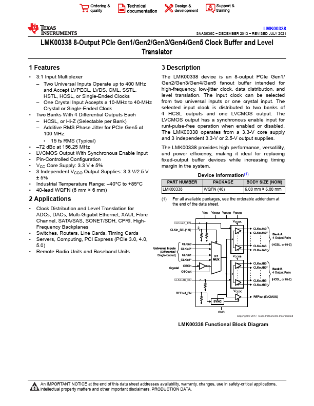
The LMK00338 device is an 8-output PCIe Gen1/ Gen2/Gen3/Gen4/Gen5 fanout buffer intended for high-frequency, low-jitter clock, data distribution, and level translation.

The input clock can be selected from two universal inputs or one crystal input.

Features

  • 3:1 Input Multiplexer.
  • Two Universal Inputs Operate up to 400 MHz and Accept LVPECL, LVDS, CML, SSTL, HSTL, HCSL, or Single-Ended Clocks.
  • One Crystal Input Accepts a 10-MHz to 40-MHz Crystal or Single-Ended Clock.
  • Two Banks With 4 Differential Outputs Each.
  • HCSL, or Hi-Z (Selectable per Bank).
  • Additive RMS Phase Jitter for PCIe Gen5 at 100 MHz:.
  • 15 fs RMS (Typical).
  • 72 dBc at 156.25 MHz.
  • LVCMOS Output With.

📥 Download Datasheet

Datasheet Details

Part number LMK00338
Manufacturer Texas Instruments
File Size 1.97 MB
Description 8-Output PCIe Gen1/Gen2/Gen3/Gen4/Gen5 Clock Buffer and Level Translator
Datasheet download datasheet LMK00338 Datasheet
Other Datasheets by Texas Instruments

Full PDF Text Transcription

Click to expand full text
LMK00338 SNAS636C – DECEMBER 2013 – REVISED JULY 2021 LMK00338 8-Output PCIe Gen1/Gen2/Gen3/Gen4/Gen5 Clock Buffer and Level Translator 1 Features • 3:1 Input Multiplexer – Two Universal Inputs Operate up to 400 MHz and Accept LVPECL, LVDS, CML, SSTL, HSTL, HCSL, or Single-Ended Clocks – One Crystal Input Accepts a 10-MHz to 40-MHz Crystal or Single-Ended Clock • Two Banks With 4 Differential Outputs Each – HCSL, or Hi-Z (Selectable per Bank) – Additive RMS Phase Jitter for PCIe Gen5 at 100 MHz: • 15 fs RMS (Typical) • –72 dBc at 156.25 MHz • LVCMOS Output With Synchronous Enable Input • Pin-Controlled Configuration • VCC Core Supply: 3.3 V ± 5% • 3 Independent VCCO Output Supplies: 3.3 V/2.
Published: |