📁 Similar Datasheet
Part Number
Description
Manufacturer
SSM3J35CT
Silicon P-Channel MOSFET
Toshiba Semiconductor
SSM3J353F
Silicon P-Channel MOSFET
Toshiba Semiconductor
SSM3J35FS
Silicon P-Channel MOSFET
Toshiba Semiconductor
SSM3J35MFV
Silicon P-Channel MOSFET
Toshiba Semiconductor
SSM3J304T
Silicon P-Channel MOSFET
Toshiba Semiconductor
Other Datasheets by Toshiba
Full PDF Text Transcription (Reference)
The following content is an automatically extracted verbatim text
from the original manufacturer datasheet and is provided for reference purposes only.
View original datasheet text
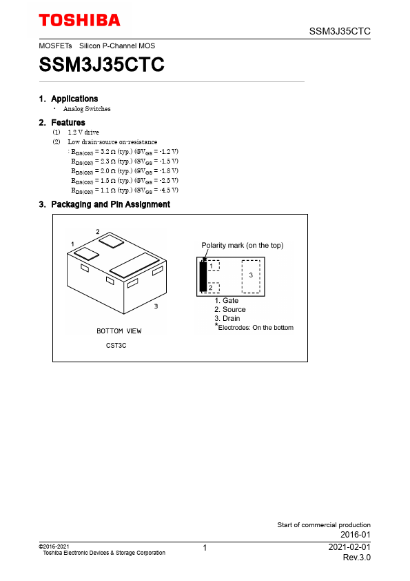
MOSFETs Silicon P-Channel MOS
SSM3J35CTC
1. Applications
• Analog Switches
2. Features
(1) 1.2 V drive (2) Low drain-source on-resistance
: RDS(ON) = 3.2 Ω (typ.) (@VGS = -1.2 V) RDS(ON) = 2.3 Ω (typ.) (@VGS = -1.5 V) RDS(ON) = 2.0 Ω (typ.) (@VGS = -1.8 V) RDS(ON) = 1.5 Ω (typ.) (@VGS = -2.5 V) RDS(ON) = 1.1 Ω (typ.) (@VGS = -4.5 V)
3. Packaging and Pin Assignment
SSM3J35CTC
CST3C
©2016-2021
1
Toshiba Electronic Devices & Storage Corporation
Start of commercial production
2016-01
2021-02-01 Rev.3.0
SSM3J35CTC
4.
 SSM3J35CTC Datasheet