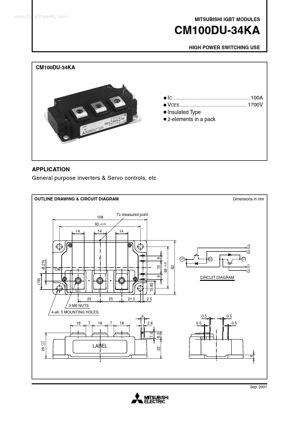
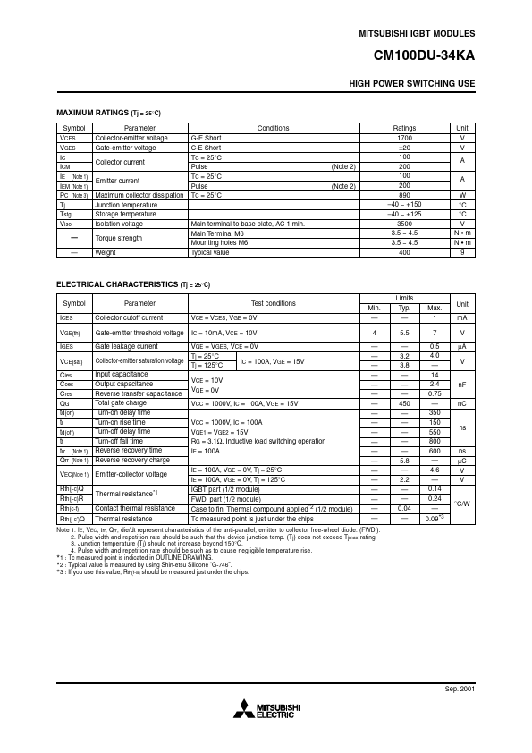
MAXIMUM RATINGS (Tj = 25°C)
Symbol
VCES
VGES
IC
ICM
IE (Note 1)
IEM (Note 1)
PC (Note 3)
Tj
Tstg
Viso
—
—
Parameter
Collector-emitter voltage
Gate-emitter voltage
Collector current
Emitter current
Maximum collector dissipation
Junction temperature
Storage temperature
Isolation voltage
Torque strength
Weight
G-E Short
C-E Short
TC = 25°C
Pulse
TC = 25°C
Pulse
TC = 25°C
Conditions
Main terminal to base plate, AC 1 min.
Main Terminal M6
Mounting holes M6
Typical value
MITSUBISHI IGBT MODULES
CM100DU-34KA
HIGH POWER SWITCHING USE
(Note 2)
(Note 2)
Ratings
1700
±20
100
200
100
200
890
–40 ~ +150
–40 ~ +125
3500
3.5 ~ 4.5
3.5 ~ 4.5
400
Unit
V
V
A
A
W
°C
°C
V
N•m
N•m
g
ELECTRICAL CHARACTERISTICS (Tj = 25°C)
Symbol
Parameter
ICES Collector cutoff current
Test conditions
VCE = VCES, VGE = 0V
Min.
—
VGE(th) Gate-emitter threshold voltage IC = 10mA, VCE = 10V
4
IGES
VCE(sat)
Cies
Coes
Cres
QG
td(on)
tr
td(off)
tf
trr (Note 1)
Qrr (Note 1)
VEC(Note 1)
Rth(j-c)Q
Rth(j-c)R
Rth(c-f)
Rth(j-c’)Q
Gate leakage current
Collector-emitter saturation voltage
Input capacitance
Output capacitance
Reverse transfer capacitance
Total gate charge
Turn-on delay time
Turn-on rise time
Turn-off delay time
Turn-off fall time
Reverse recovery time
Reverse recovery charge
Emitter-collector voltage
Thermal resistance*1
Contact thermal resistance
Thermal resistance
VGE = VGES, VCE = 0V
Tj = 25°C
Tj = 125°C
IC = 100A, VGE = 15V
VCE = 10V
VGE = 0V
VCC = 1000V, IC = 100A, VGE = 15V
VCC = 1000V, IC = 100A
VGE1 = VGE2 = 15V
RG = 3.1Ω, Inductive load switching operation
IE = 100A
IE = 100A, VGE = 0V, Tj = 25°C
IE = 100A, VGE = 0V, Tj = 125°C
IGBT part (1/2 module)
FWDi part (1/2 module)
Case to fin, Thermal compound applied*2 (1/2 module)
Tc measured point is just under the chips
—
—
—
—
—
—
—
—
—
—
—
—
—
—
—
—
—
—
—
Note 1. IE, VEC, trr, Qrr, die/dt represent characteristics of the anti-parallel, emitter to collector free-wheel diode. (FWDi).
2. Pulse width and repetition rate should be such that the device junction temp. (Tj) does not exceed Tjmax rating.
3. Junction temperature (Tj) should not increase beyond 150°C.
4. Pulse width and repetition rate should be such as to cause negligible temperature rise.
*1 : Tc measured point is indicated in OUTLINE DRAWING.
*2 : Typical value is measured by using Shin-etsu Silicone “G-746”.
*3 : If you use this value, Rth(f-a) should be measured just under the chips.
Limits
Typ.
—
5.5
—
3.2
3.8
—
—
—
450
—
—
—
—
—
5.8
—
2.2
—
—
0.04
—
Max.
1
Unit
mA
7
0.5
4.0
—
14
2.4
0.75
—
350
150
550
800
600
—
4.6
—
0.14
0.24
—
0.09*3
V
µA
V
nF
nC
ns
ns
µC
V
V
°C/W
Sep. 2001