Features
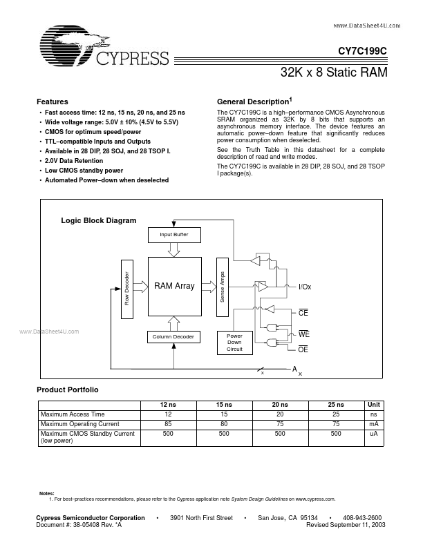
• Fast access time: 12 ns, 15 ns, 20 ns, and 25 ns
• Wide voltage range: 5.0V ± 10% (4.5V to 5.5V)
• CMOS for optimum speed/power
• TTL–compatible Inputs and Outputs
• Available in 28 DIP, 28 SOJ, and 28 TSOP I.
• 2.0V Data Retention
• Low CMOS standby power
• Automated Power–down when deselected
CY7C199C
32K x 8 Static RAM
General Description1
The CY7C199C is a high–performance CMOS Asynchronous
SRAM organized as 32K by 8 bits that supports an
asynchronous memory interface. The device features an
automatic power–down feature that significantly reduces
power consumption when deselected.
See the Truth Table in this datasheet for a complete
description of read and write modes.
The CY7C199C is available in 28 DIP, 28 SOJ, and 28 TSOP
I package(s).
Logic Block Diagram
Input Buffer
RAM Array
I/Ox
www.DataSheet4U.com
Column Decoder
Product Portfolio
Maximum Access Time
Maximum Operating Current
Maximum CMOS Standby Current
(low power)
12 ns
12
85
500
Power
Down
Circuit
X
CE
WE
OE
A
X
15 ns
15
80
500
20 ns
20
75
500
25 ns
25
75
500
Unit
ns
mA
uA
Notes:
1. For best–practices recommendations, please refer to the Cypress application note System Design Guidelines on www.cypress.com.
Cypress Semiconductor Corporation • 3901 North First Street • San Jose, CA 95134 • 408-943-2600
Document #: 38-05408 Rev. *A
Revised September 11, 2003