Datasheet4U Logo Datasheet4U.com

SN74LVC2GU04 - Dual Inverter Gate

Description

This dual inverter is designed for 1.65-V to 5.5-V VCC operation.

The SN74LVC2GU04 device contains two inverters with unbuffered outputs and performs the Boolean function Y = A.

NanoFree™ package technology is a major breakthrough in IC packaging concepts, using the die as the package.

Features

  • 1.
  • 2 Available in the Texas Instruments NanoFree™ Package.
  • Supports 5-V VCC Operation.
  • Inputs Accept Voltages to 5.5 V.
  • Max tpd of 3.7 ns at 3.3 V.
  • Low Power Consumption, 10-µA Max ICC.
  • ±24-mA Output Drive at 3.3 V.
  • Typical VOLP (Output Ground Bounce) 2 V at VCC = 3.3 V, TA = 25°C.
  • Ioff Supports Live Insertion, Partial-PowerDown Mode, and Back-Dr.

📥 Download Datasheet

Full PDF Text Transcription

Click to expand full text
SN74LVC2GU04 www.ti.com SCES197N – APRIL 1999 – REVISED DECEMBER 2013
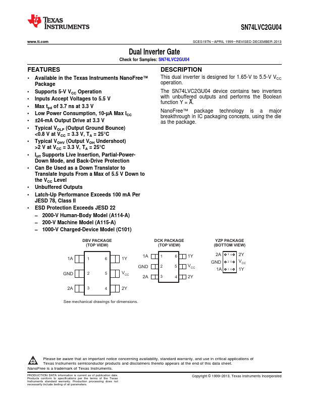
 Dual Inverter Gate Check for Samples: SN74LVC2GU04 FEATURES 1 •2 Available in the Texas Instruments NanoFree™ Package • Supports 5-V VCC Operation • Inputs Accept Voltages to 5.5 V • Max tpd of 3.7 ns at 3.3 V • Low Power Consumption, 10-µA Max ICC • ±24-mA Output Drive at 3.3 V • Typical VOLP (Output Ground Bounce) <0.8 V at VCC = 3.3 V, TA = 25°C • Typical VOHV (Output VOH Undershoot) >2 V at VCC = 3.3 V, TA = 25°C • Ioff Supports Live Insertion, Partial-PowerDown Mode, and Back-Drive Protection • Can Be Used as a Down Translator to Translate Inputs From a Max of 5.
Published: |