Datasheet Details
| Part number | SN74LVC2G04 |
|---|---|
| Manufacturer | Texas Instruments |
| File Size | 1.32 MB |
| Description | Dual Inverter Gate |
| Datasheet |
 SN74LVC2G04 Datasheet SN74LVC2G04 Datasheet
|
|
|
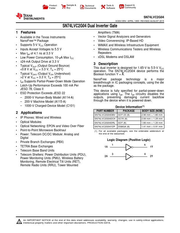
This dual inverter is designed for 1.65-V to 5.5-V VCC operation.
The SN74LVC2G04 device performs the Boolean function Y = A.
NanoFree package technology is a major breakthrough in IC packaging concepts, using the die as the package.
| Part number | SN74LVC2G04 |
|---|---|
| Manufacturer | Texas Instruments |
| File Size | 1.32 MB |
| Description | Dual Inverter Gate |
| Datasheet |
SN74LVC2G04 Datasheet
|
|
|
|
| Part Number | Description | Manufacturer |
|---|---|---|
| SN74LVC1G125 | high performance non-inverting buffer | UMW |
| SN74LVC1G34 | Single buffer | UMW |
| SN74L71 | AND-Gate R-S Master-Slave F-F | National Semiconductor |
| SN74L74N | Dual D-Type Flip-Flop | ETC |
| SN74LS00 | QUAD 2-INPUT NAND GATE | Motorola |
| Part Number | Description |
|---|---|
| SN74LVC2G04-EP | Dual Inverter Gate |
| SN74LVC2G00 | Dual 2-Input Positive-NAND Gate |
| SN74LVC2G00W-EP | DUAL 2-INPUT POSITIVE-NAND GATE |
| SN74LVC2G02 | Dual 2-Input Positive-NOR Gate |
| SN74LVC2G02-EP | Dual 2-Input Positive-NOR Gate |