Datasheet4U Logo Datasheet4U.com

CDCVF310 - 2.5-V TO 3.3-V HIGH-PERFORMANCE CLOCK BUFFER

Datasheet Summary

Description

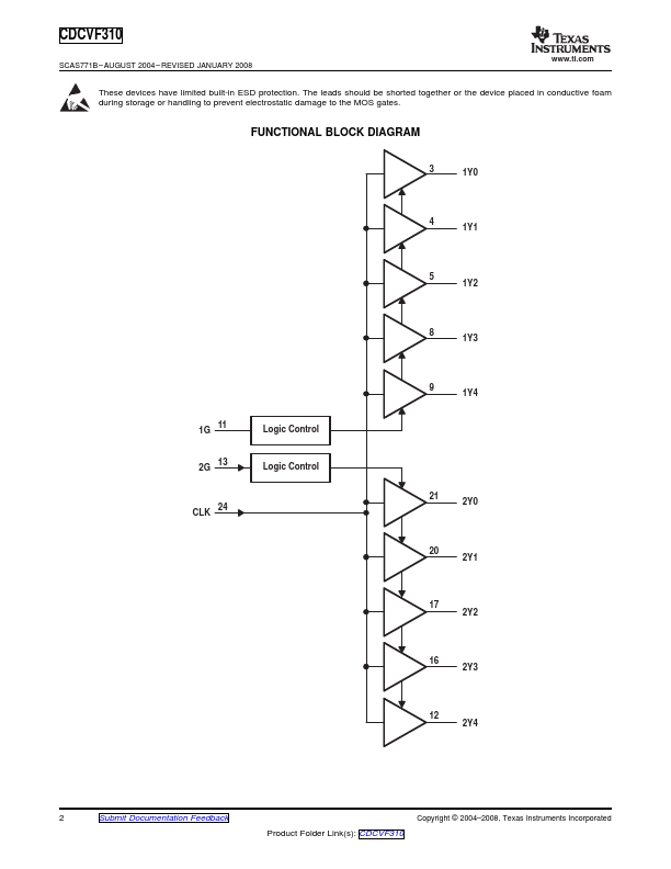
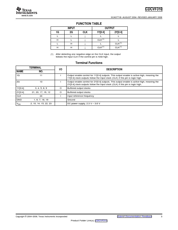
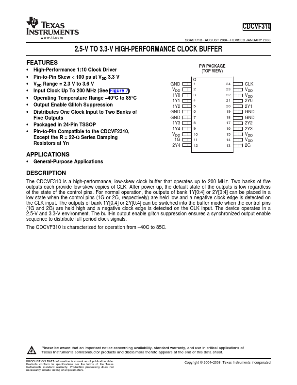
The CDCVF310 is a high-performance, low-skew clock buffer that operates up to 200 MHz.

Two banks of five outputs each provide low-skew copies of CLK.

After power up, the default state of the outputs is low regardless of the state of the control pins.

Features

  • 1.
  • High-Performance 1:10 Clock Driver.
  • Pin-to-Pin Skew < 100 ps at VDD 3.3 V.
  • VDD Range = 2.3 V to 3.6 V.
  • Input Clock Up To 200 MHz (See Figure 7).
  • Operating Temperature Range.
  • 40°C to 85°C.
  • Output Enable Glitch Suppression.
  • Distributes One Clock Input to Two Banks of Five Outputs.
  • Packaged in 24-Pin TSSOP.
  • Pin-to-Pin Compatible to the CDCVF2310, Except the R = 22-Ω Series Damping Resistors at Yn.

📥 Download Datasheet

Datasheet preview – CDCVF310

Datasheet Details

Part number CDCVF310
Manufacturer Texas Instruments
File Size 417.27 KB
Description 2.5-V TO 3.3-V HIGH-PERFORMANCE CLOCK BUFFER
Datasheet download datasheet CDCVF310 Datasheet
Additional preview pages of the CDCVF310 datasheet.
Other Datasheets by Texas Instruments

Full PDF Text Transcription

Click to expand full text
www.ti.com CDCVF310 SCAS771B – AUGUST 2004 – REVISED JANUARY 2008 2.5-V TO 3.3-V HIGH-PERFORMANCE CLOCK BUFFER FEATURES 1 • High-Performance 1:10 Clock Driver • Pin-to-Pin Skew < 100 ps at VDD 3.3 V • VDD Range = 2.3 V to 3.
Published: |