Datasheet4U Logo Datasheet4U.com

CDCLVP1102 - High-Performance Clock Buffer

Datasheet Summary

Description

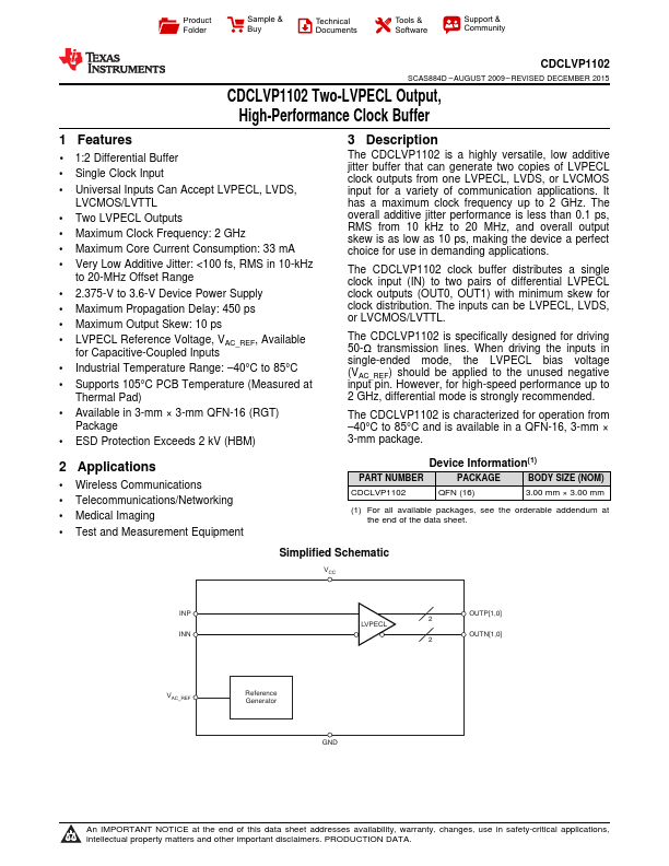
The CDCLVP1102 is a highly versatile, low additive jitter buffer that can generate two copies of LVPECL clock outputs from one LVPECL, LVDS, or LVCMOS input for a variety of communication applications.

It has a maximum clock frequency up to 2 GHz.

Features

  • 1 1:2 Differential Buffer.
  • Single Clock Input.
  • Universal Inputs Can Accept LVPECL, LVDS, LVCMOS/LVTTL.
  • Two LVPECL Outputs.
  • Maximum Clock Frequency: 2 GHz.
  • Maximum Core Current Consumption: 33 mA.
  • Very Low Additive Jitter:.

📥 Download Datasheet

Datasheet preview – CDCLVP1102

Datasheet Details

Part number CDCLVP1102
Manufacturer Texas Instruments
File Size 1.33 MB
Description High-Performance Clock Buffer
Datasheet download datasheet CDCLVP1102 Datasheet
Additional preview pages of the CDCLVP1102 datasheet.
Other Datasheets by Texas Instruments

Full PDF Text Transcription

Click to expand full text
Product Folder Sample & Buy Technical Documents Tools & Software Support & Community CDCLVP1102 SCAS884D – AUGUST 2009 – REVISED DECEMBER 2015 CDCLVP1102 Two-LVPECL Output, High-Performance Clock Buffer 1 Features •1 1:2 Differential Buffer • Single Clock Input • Universal Inputs Can Accept LVPECL, LVDS, LVCMOS/LVTTL • Two LVPECL Outputs • Maximum Clock Frequency: 2 GHz • Maximum Core Current Consumption: 33 mA • Very Low Additive Jitter: <100 fs, RMS in 10-kHz to 20-MHz Offset Range • 2.375-V to 3.
Published: |