Click to expand full text
• Contains Four Flip-Flops with Double-Rail
Outputs
• Clock Enable Latched to Avoid False
Clocking
• Applications Include: Buffer/Storage
Registers, Shift Registers, Pattern
Generators
• Flow-Through Architecture Optimizes PCB
Layout
• Center-Pin VCC and GND Pin
Configurations Minimize High-Speed
Switching Noise
• EPIC (Enhanced-Performance Implanted
CMOS) 1-µm Process
• 500-mA Typical Latch-Up Immunity at
125°C
• Package Options Include Plastic
Small-Outline Packages and Standard
Plastic 300-mil DIPs
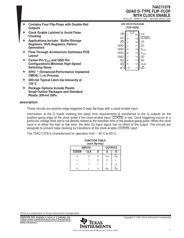
74AC11379 QUAD D-TYPE FLIP-FLOP
WITH CLOCK ENABLE
SCAS104 − MARCH 1990 − REVISED APRIL 1993
DW OR N PACKAGE (TOP VIEW)
1Q 2Q 2Q GND GND GND GND 3Q 3Q 4Q
1 2 3 4 5 6 7 8 9 10
20 1Q 19 CLKEN 18 1D 17 2D
16 VCC 15 VCC 14 3D 13 4D 12 CLK 11 4Q
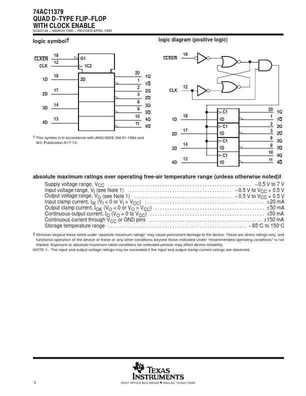
description
These circuits are positive-edge-t
 74AC11379 Datasheet