Click to expand full text
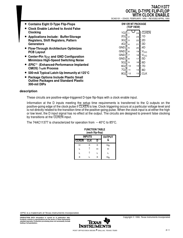
• Contains Eight D-Type Flip-Flops • Clock Enable Latched to Avoid False
Clocking
• Applications Include: Buffer/Storage
Registers, Shift Registers, Pattern
Generators
• Flow-Through Architecture Optimizes
PCB Layout
• Center-Pin VCC and GND Configuration
Minimizes High-Speed Switching Noise
t• EPIC (Enhanced-Performance Implanted CMOS) 1-mm Process
• 500-mA Typical Latch-Up Immunity at 125°C • Package Options Include Plastic Small
Outline Packages and Standard Plastic
300-mil DIPs
74AC11377 OCTAL D-TYPE FLIP-FLOP
WITH CLOCK ENABLE
SCAS101 – D3420, FEBRUARY 1990 – REVISED APRIL 1993
DW OR NT PACKAGE (TOP VIEW)
1Q 2Q 3Q 4Q GND GND GND GND 5Q 6Q 7Q 8Q
1 2 3 4 5 6 7 8 9 10 11 12
24 CLKEN 23 1D 22 2D 21 3D 20 4D 19 VCC 18 VCC 17 5D
16 6D
15 7D 14 8D 13 CLK
description
These circuits are
 74AC11377 Datasheet