Click to expand full text
P0903BDG
N-Channel Enhancement Mode MOSFET
PRODUCT SUMMARY
V(BR)DSS
RDS(ON)
ID
25V
9.5mΩ @VGS = 10V
56A
TO-252
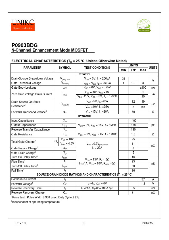
ABSOLUTE MAXIMUM RATINGS (TC = 25 °C Unless Otherwise Noted)
PARAMETERS/TEST CONDITIONS
SYMBOL
LIMITS
Drain-Source Voltage
VDS
25
Gate-Source Voltage
VGS
±20
Continuous Drain Current Pulsed Drain Current1
TC= 25 °C TC= 100 °C
ID
56 35
IDM
160
Avalanche Current
IAS
34
Avalanche Energy
L=0.1mH
EAS
60
Power Dissipation
TC= 25 °C TC= 100°C
PD
49 20
Junction & Storage Temperature Range
Tj, Tstg
-55 to 150
Lead Temperature (1/16” from case for 10 sec.)
TL
275
UNITS V
A
mJ W °C
THERMAL RESISTANCE RATINGS
THERMAL RESISTANCE Junction-to-Case Junction-to-Ambient 1Pulse width limited by maximum junction temperature.
 P0903BDG Datasheet