Click to expand full text
NIKO-SEM
N-Channel Logic Level Enhancement Mode Field Effect Transistor
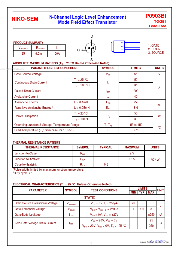
D
P0903BI
TO-251 Lead-Free
PRODUCT SUMMARY V(BR)DSS 25 RDS(ON) 9.5m£[ ID 50A
3
G S
1. GATE 2. DRAIN 3. SOURCE
ABSOLUTE MAXIMUM RATINGS (TC = 25 °C Unless Otherwise Noted)
www.DataSheet4U.com
PARAMETERS/TEST CONDITIONS
SYMBOL VGS
1 2
LIMITS ±20 50 35
UNITS V
Gate-Source Voltage Continuous Drain Current Pulsed Drain Current 1 Avalanche Current Avalanche Energy Repetitive Avalanche Energy Power Dissipation
2
TC = 25 °C TC = 100 °C
ID IDM IAR
A
200 40 250 8.6 50 30 W mJ
L = 0.1mH L = 0.05mH TC = 25 °C TC = 100 °C
EAS EAR PD Tj, Tstg TL
Operating Junction & Storage Temperature Range Lead Temperature (1/16” from case for 10 sec.
 P0903BI Datasheet