Datasheet Details
| Part number | NB3L553 |
|---|---|
| Manufacturer | Onsemi |
| File Size | 273.40 KB |
| Description | 2.5V / 3.3V / 5.0V 1:4 Clock Fanout Buffer |
| Datasheet |
 NB3L553 Datasheet NB3L553 Datasheet
|
|
|
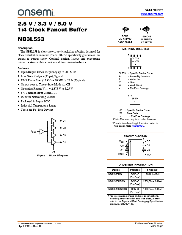
clock distribution in mind.
tooutput skew.
Optimal design, layout and processing minimize skew within a device and from device to device.
| Part number | NB3L553 |
|---|---|
| Manufacturer | Onsemi |
| File Size | 273.40 KB |
| Description | 2.5V / 3.3V / 5.0V 1:4 Clock Fanout Buffer |
| Datasheet |
NB3L553 Datasheet
|
|
|
|