Datasheet Details
| Part number | NB3L8504S |
|---|---|
| Manufacturer | Onsemi |
| File Size | 246.12 KB |
| Description | 2.5V / 3.3V 1:4 Differential Input to LVDS Fanout Buffer / Translator |
| Datasheet |
 NB3L8504S Datasheet NB3L8504S Datasheet
|
|
|
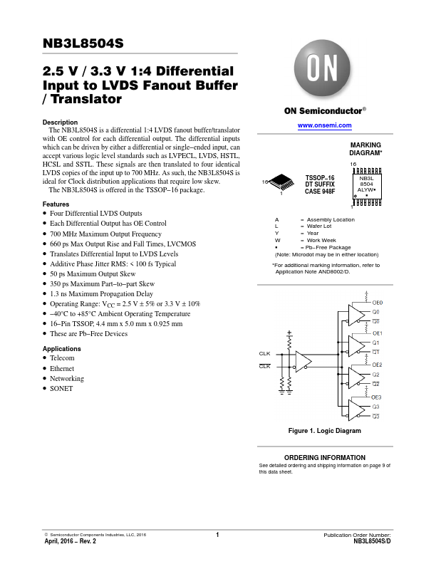
with OE control for each differential output.
ended input, can accept various logic level standards such as LVPECL, LVDS, HSTL, HCSL and SSTL.
| Part number | NB3L8504S |
|---|---|
| Manufacturer | Onsemi |
| File Size | 246.12 KB |
| Description | 2.5V / 3.3V 1:4 Differential Input to LVDS Fanout Buffer / Translator |
| Datasheet |
NB3L8504S Datasheet
|
|
|
|