Datasheet4U Logo Datasheet4U.com

NB3L8543S - 2.5V/3.3V Differential 2:1 MUX to 4 LVDS Clock Fanout Buffer Outputs

Description

The NB3L8543S is a high performance, low skew 1 to

Clock Fanout Buffer.

Features

  • a multiplexed input which can be driven by either a differential or single.
  • ended input to allow for the distribution of a lower speed clock along with the high speed system clock. The CLK_SEL pin will select the differential CLK and CLK inputs when LOW (or left open and pulled LOW by the internal pull.
  • down resistor). When CLK_SEL is HIGH, the differential PCLK and PCLK inputs are selected. The common clock enable pin, CLK_EN, is synchronous so that the outputs will only be enable.

📥 Download Datasheet

Datasheet preview – NB3L8543S

Datasheet Details

Part number NB3L8543S
Manufacturer Onsemi
File Size 231.18 KB
Description 2.5V/3.3V Differential 2:1 MUX to 4 LVDS Clock Fanout Buffer Outputs
Datasheet download datasheet NB3L8543S Datasheet
Additional preview pages of the NB3L8543S datasheet.
Other Datasheets by ON Semiconductor

Full PDF Text Transcription

Click to expand full text
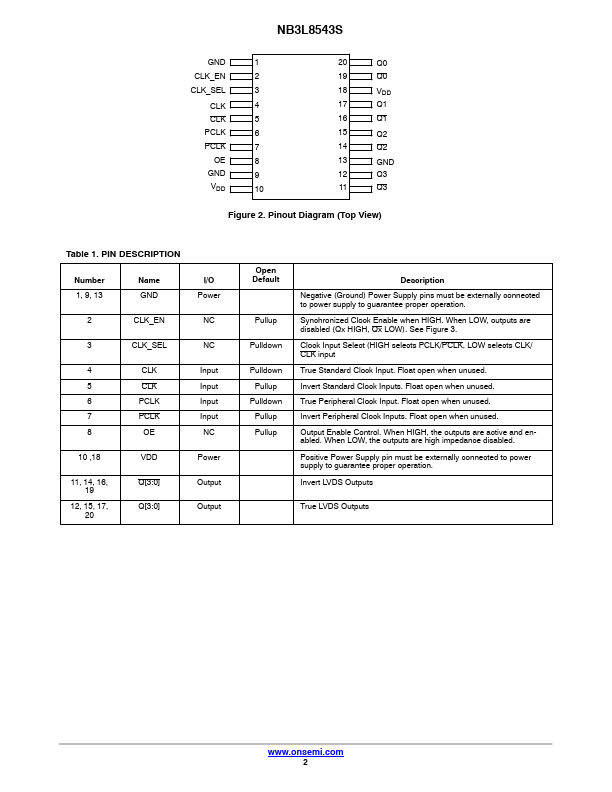
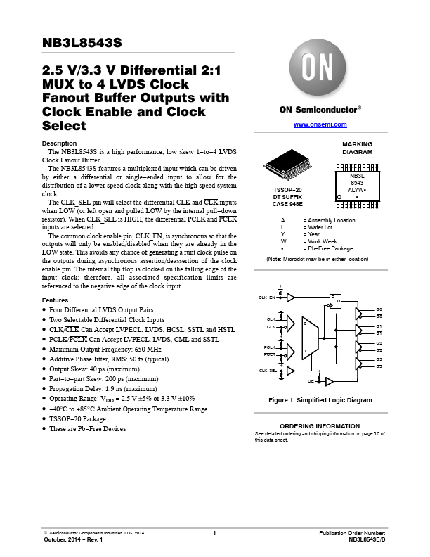
NB3L8543S 2.5 V/3.3 V Differential 2:1 MUX to 4 LVDS Clock Fanout Buffer Outputs with Clock Enable and Clock Select Description The NB3L8543S is a high performance, low skew 1−to−4 LVDS Clock Fanout Buffer. The NB3L8543S features a multiplexed input which can be driven by either a differential or single−ended input to allow for the distribution of a lower speed clock along with the high speed system clock. The CLK_SEL pin will select the differential CLK and CLK inputs when LOW (or left open and pulled LOW by the internal pull−down resistor). When CLK_SEL is HIGH, the differential PCLK and PCLK inputs are selected. 
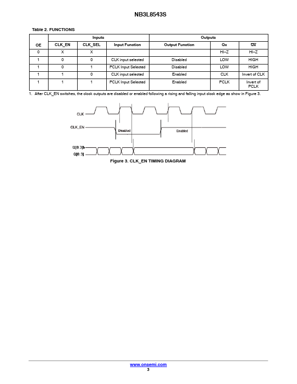
The common clock enable pin, CLK_EN, is synchronous so that the outputs will only be enabled/disabled when they are already in the LOW state.
Published: |