Datasheet Details
| Part number | K3366 |
|---|---|
| Manufacturer | NEC (now Renesas Electronics) |
| File Size | 160.28 KB |
| Description | 2SK3366 |
| Datasheet |
 K3366 Datasheet K3366 Datasheet
|
|
|
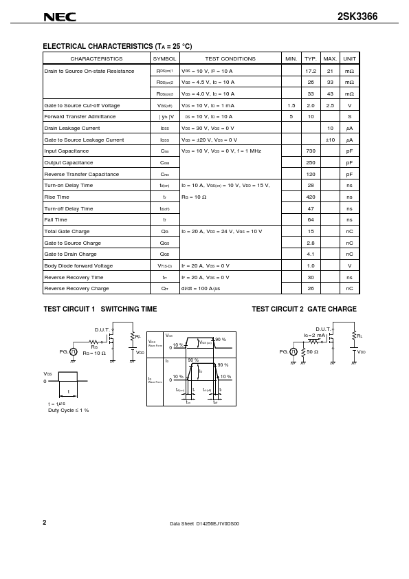
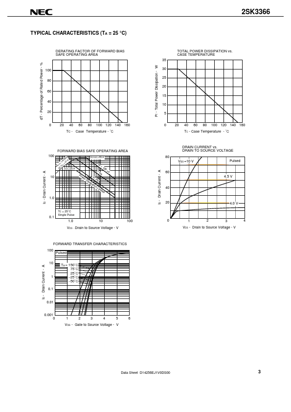
The 2SK3366 is N -Channel M OS Field Effect T ransistor designed for D C/DC converter application of notebook computers.
| Part number | K3366 |
|---|---|
| Manufacturer | NEC (now Renesas Electronics) |
| File Size | 160.28 KB |
| Description | 2SK3366 |
| Datasheet |
K3366 Datasheet
|
|
|
|
Note: Below is a high-fidelity text extraction (approx. 800 characters) for K3366. For precise diagrams, and layout, please refer to the original PDF.
DATA SHEET MOS FIELD EFFECT TRANSISTOR 2SK3366 SWITCHING N-CHANNEL POWER MOS FET INDUSTRIAL USE DESCRIPTION The 2SK3366 is N -Channel M OS Field Effect T ransistor design...
| Part Number | Description |
|---|---|
| K3365 | 2SK3365 |
| K3304 | 2SK3304 |
| K3306 | SWITCHING N-CHANNEL POWER MOS FET |
| K3307 | SWITCHING N-CHANNEL POWER MOSFET |
| K3322 | 2SK3322 |
| K3324 | 2SK3324 |
| K3326 | 2SK3326 |
| K3353 | 2SK3353 |
| K3377 | 2SK3377 |
| K3385 | 2SK3385 |