Note: Below is a high-fidelity text extraction (approx. 800 characters) for
BS170. For precise diagrams, and layout, please refer to the original PDF.
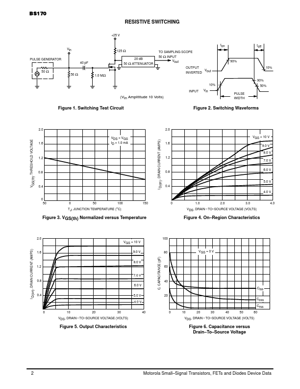
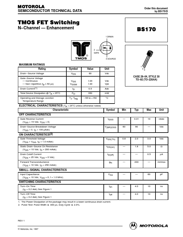
MOTOROLA SEMICONDUCTOR TECHNICAL DATA Order this document by BS170/D TMOS FET Switching N–Channel — Enhancement 1 DRAIN BS170 2 GATE 3 SOURCE ® MAXIMUM RATINGS Rating Dra...
View more extracted text
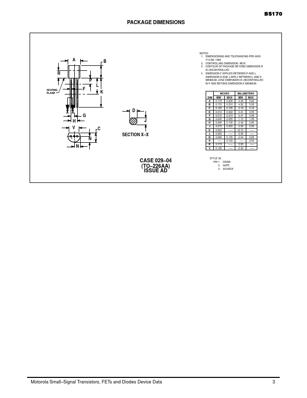
Enhancement 1 DRAIN BS170 2 GATE 3 SOURCE ® MAXIMUM RATINGS Rating Drain – Source Voltage Gate–Source Voltage — Continuous — Non–repetitive (tp ≤ 50 µs) Drain Current(1) Total Device Dissipation @ TA = 25°C Operating and Storage Junction Temperature Range Symbol VDS VGS VGSM ID PD TJ, Tstg Value 60 ± 20 ± 40 0.5 350 1 Unit Vdc Vdc Vpk Adc mW °C 2 3 CASE 29–04, STYLE 30 TO–92 (TO–226AA) – 55 to +150 ELECTRICAL CHARACTERISTICS (TA = 25°C unless otherwise noted) Characteristic Symbol Min Typ Max Unit OFF CHARACTERISTICS Gate Reverse Current (VGS = 15 Vdc, VDS = 0) Drain–Source Breakdown Voltage (VGS = 0, ID = 100 µAdc) IGSS V
 BS170 Datasheet