Click to expand full text
www.DataSheet4U.com
64Mb DDR SDRAM
H5DU6462CTR
This document is a general product description and is subject to change without notice. Hynix Semiconductor does not assume any responsibility for use of circuits described. No patent licenses are implied. Rev. 1.0 /July. 2008 1
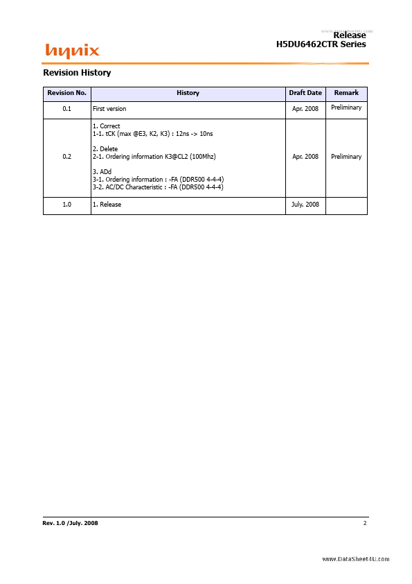
Release H5DU6462CTR Series Revision History
Revision No. 0.1 First version 1. Correct 1-1. tCK (max @E3, K2, K3) : 12ns -> 10ns 0.2 2. Delete 2-1. Ordering information K3@CL2 (100Mhz) 3. ADd 3-1. Ordering information : -FA (DDR500 4-4-4) 3-2. AC/DC Characteristic : -FA (DDR500 4-4-4) 1.0 1. Release July. 2008 Apr. 2008 Preliminary History Draft Date Apr. 2008 Remark Preliminary
www.DataSheet4U.com
Rev. 1.0 /July. 2008
2
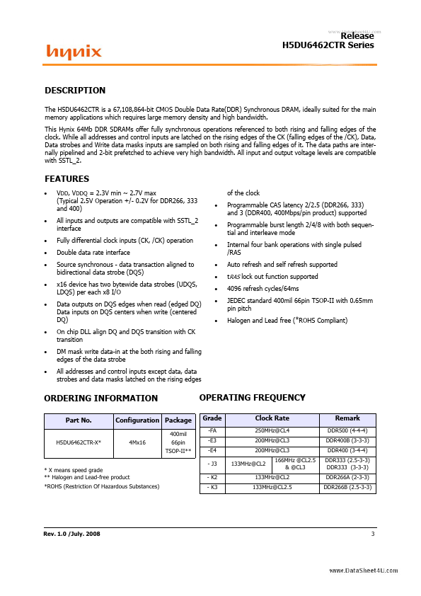
Release H5DU6462CTR Series
www.DataSheet4U.
 H5DU6462CTR Datasheet