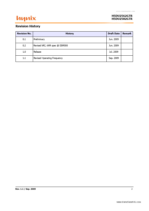
Datasheet Details
| Part number | H5DU2582GTR |
|---|---|
| Manufacturer | SK Hynix |
| File Size | 425.37 KB |
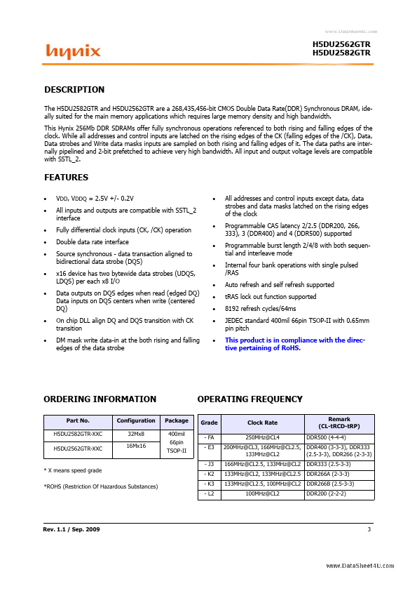
| Description | (H5DU2562GTR / H5DU2582GTR) 256Mb DDR SDRAM |
| Datasheet |
 H5DU2582GTR Datasheet H5DU2582GTR Datasheet
|
|
|
Download the H5DU2582GTR datasheet PDF. This datasheet also covers the H5DU2562GTR variant, as both devices belong to the same (h5du2562gtr / h5du2582gtr) 256mb ddr sdram family and are provided as variant models within a single manufacturer datasheet.
and is subject to change without notice.
Hynix Semiconductor does not assume any responsibility for use of circuits described.
No patent licenses are implied.
| Part number | H5DU2582GTR |
|---|---|
| Manufacturer | SK Hynix |
| File Size | 425.37 KB |
| Description | (H5DU2562GTR / H5DU2582GTR) 256Mb DDR SDRAM |
| Datasheet |
H5DU2582GTR Datasheet
|
|
|
|
| Part Number | Description | Manufacturer |
|---|
| Part Number | Description |
|---|---|
| H5DU2562GFR | 256Mb DDR SDRAM |
| H5DU2562GTR | (H5DU2562GTR / H5DU2582GTR) 256Mb DDR SDRAM |
| H5DU1262GTR | 128Mb DDR SDRAM |
| H5DU5162EFR | (H5DU5162EFR / H5DU5182EFR) 512Mb DDR SDRAM |
| H5DU5162ETR | (H5DU5162ETR / H5DU5182ETR) 512Mb DDR SDRAM |