Click to expand full text
www.DataSheet4U.com
256Mb DDR SDRAM
H5DU2562GTR H5DU2582GTR
This document is a general product description and is subject to change without notice. Hynix Semiconductor does not assume any responsibility for use of circuits described. No patent licenses are implied. Rev. 1.1 / Sep. 2009 1
www.DataSheet4U.com
H5DU2562GTR H5DU2582GTR
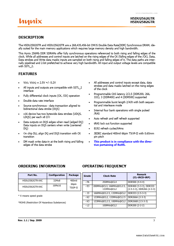
Revision History
Revision No. 0.1 0.2 1.0 1.1 Preliminary Revised tRC, tWR spec @ DDR500 Release Revised Operating Frequency History Draft Date Jun. 2009 Jun. 2009 Jul. 2009 Sep. 2009 Remark
Rev. 1.1 / Sep. 2009
2
www.DataSheet4U.
 H5DU2562GTR Datasheet