Click to expand full text
CY7C1316KV18, CY7C1916KV18 CY7C1318KV18, CY7C1320KV18
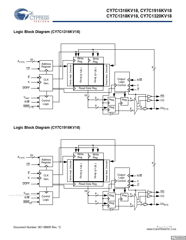
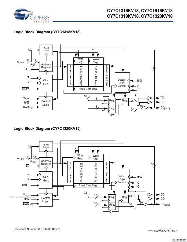
18-Mbit DDR II SRAM Two-Word Burst Architecture
18-Mbit DDR II SRAM Two-Word Burst Architecture
Features
■ ■ ■ ■ ■
Configurations
CY7C1316KV18 – 2 M × 8 CY7C1916KV18 – 2 M × 9 CY7C1318KV18 – 1 M × 18 CY7C1320KV18 – 512 K × 36
18-Mbit density (2 M × 8, 2 M × 9, 1 M × 18, 512 K × 36) 333-MHz clock for high bandwidth Two-word burst for reducing address bus frequency Double data rate (DDR) interfaces (data transferred at 666 MHz) at 333 MHz Two input clocks (K and K) for precise DDR timing ❐ SRAM uses rising edges only Two input clocks for output data (C and C) to minimize clock skew and flight time mismatches Echo clocks (CQ and CQ) simplify data capture in high-speed systems Synchronous internally self-timed writes DDR II operate
 CY7C1320KV18 Datasheet