Datasheet Details
| Part number | CY7C1320JV18 |
|---|---|
| Manufacturer | Cypress (Infineon) |
| File Size | 660.79 KB |
| Description | 18-Mbit DDR-II SRAM 2-Word Burst Architecture |
| Datasheet |
 CY7C1320JV18 Datasheet CY7C1320JV18 Datasheet
|
|
|
Download the CY7C1320JV18 datasheet PDF. This datasheet also covers the CY7C1316JV18 variant, as both devices belong to the same 18-mbit ddr-ii sram 2-word burst architecture family and are provided as variant models within a single manufacturer datasheet.
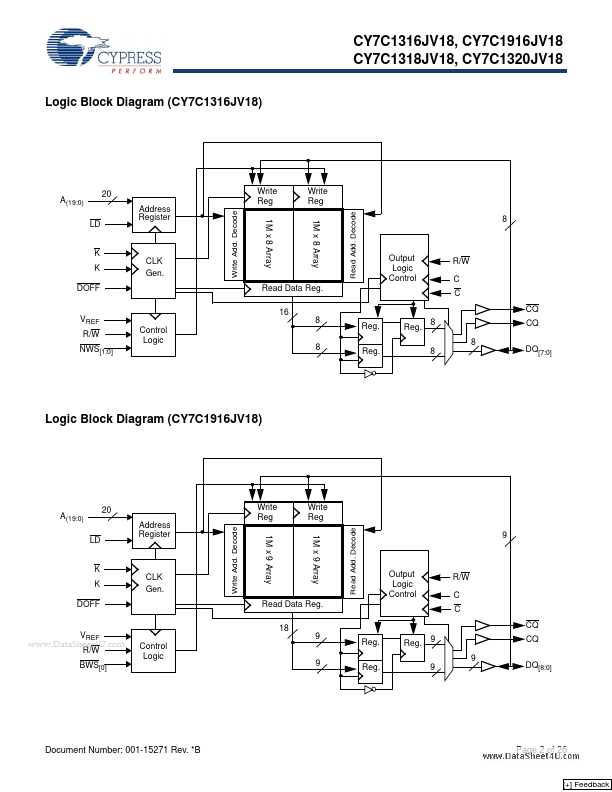
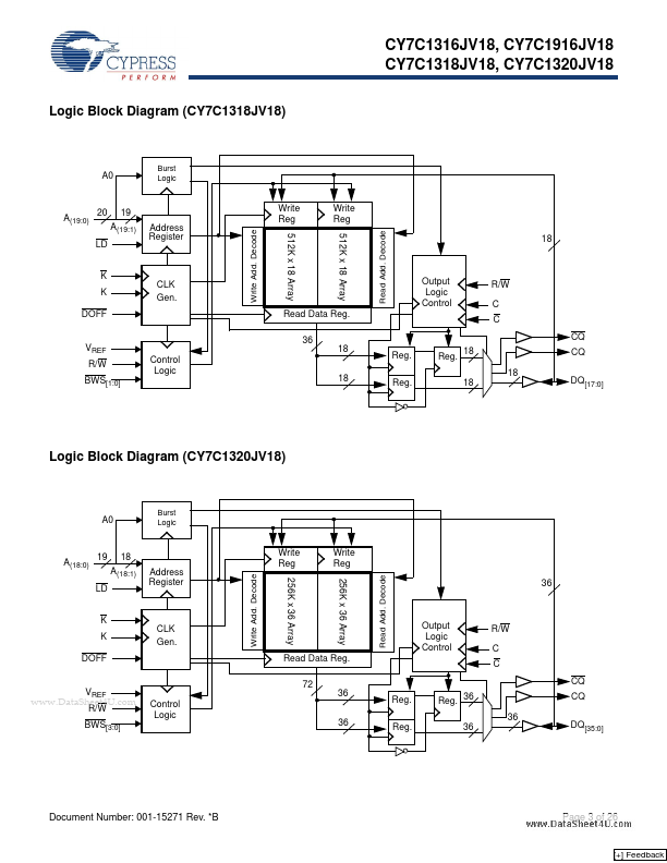
The CY7C1316JV18, CY7C1916JV18, CY7C1318JV18, and CY7C1320JV18 are 1.8V Synchronous Pipelined SRAMs equipped with DDR-II architecture.
The DDR-II consists of an SRAM core with advanced synchronous peripheral circuitry and a one-bit burst counter.
| Part number | CY7C1320JV18 |
|---|---|
| Manufacturer | Cypress (Infineon) |
| File Size | 660.79 KB |
| Description | 18-Mbit DDR-II SRAM 2-Word Burst Architecture |
| Datasheet |
CY7C1320JV18 Datasheet
|
|
|
|
| Part Number | Description | Manufacturer |
|---|---|---|
| CY7C131AE | 1K/2K x 8 Dual-Port Static RAM | Cypress |
| CY7C131E | 1K/2K x 8 Dual-Port Static RAM | Cypress |
| CY7C136AE | 1K/2K x 8 Dual-Port Static RAM | Cypress |
| CY7C136E | 1K/2K x 8 Dual-Port Static RAM | Cypress |
| CY7C1370C | 512K x 36/1M x 18 Pipelined SRAM with NoBL Architecture | Cypress |
| Part Number | Description |
|---|---|
| CY7C1320AV18 | 18-Mbit DDR-II SRAM 2-Word Burst Architecture |
| CY7C1320BV18 | 18-Mbit DDR-II SRAM 2-Word Burst Architecture |
| CY7C1320CV18 | (CY7C1xxxCV18) 18-Mbit DDR-II SRAM 2-Word Burst Architecture |
| CY7C1320KV18 | 18-Mbit DDR II SRAM Two-Word Burst Architecture |
| CY7C132 | 2K x 8 Dual-Port Static RAM |